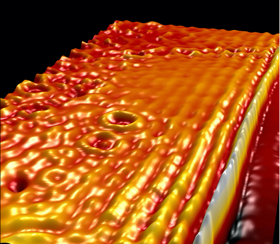
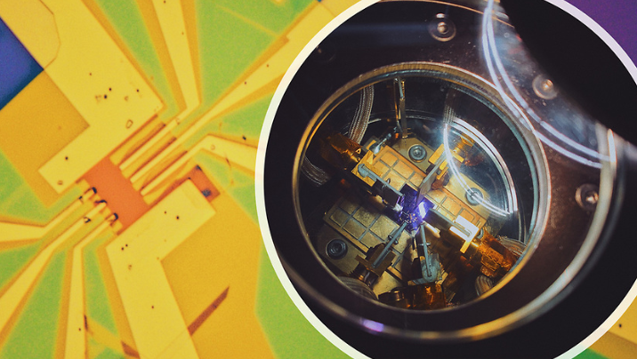
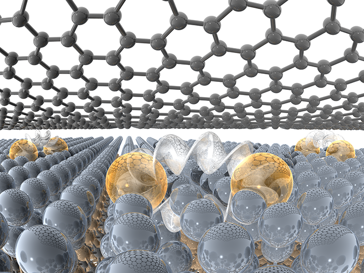
Researchers have taken the first atomic-resolution images and demonstrated electrical control of a chiral interface state – an exotic quantum phenomenon that could help researchers advance quantum computing and energy-efficient electronics.
Tag: Graphene
First human trial shows ‘wonder’ material can be developed safely
A revolutionary nanomaterial with huge potential to tackle multiple global challenges could be developed further without acute risk to human health, research suggests.
New adhesive tape picks up and sticks down 2D materials as easily as child’s play
Materials just atoms in thickness, known as two-dimensional (2D) materials, are set to revolutionize future technology, including in the electronics industry.
Researchers demonstrate a high-speed electrical readout method for graphene nanodevices
The ‘wonder material’ graphene is well-known for its high electrical conductivity, mechanical strength, and flexibility.
Scientists discover ‘flipping’ layers in heterostructures to cause changes in their properties
Transition metal dichalcogenide (TMD) semiconductors are special materials that have long fascinated researchers with their unique properties.

Graphene addition for enhancing the critical current density of Bi-2223 superconductors
Superconductors are materials that offer zero electric resistance to the flow of current on being cooled down below a certain critical temperature. Typically, superconductors have a very low critical temperature, close to absolute zero.
“Countercation engineering” for thermoresponsive graphene-oxide nanosheets
Graphene-based two-dimensional materials have recently emerged as a focus of scientific exploration due to their exceptional structural, mechanical, electrical, optical, and thermal properties.

Ribbons of graphene push the material’s potential
Think you know everything about a material? Try giving it a twist—literally. That’s the main idea of an emerging field in condensed matter physics called “twistronics,” which has researchers drastically changing the properties of 2D materials, like graphene, with subtle changes—as small as going from a 1.1° to 1.2°—in the angle between stacked layers.
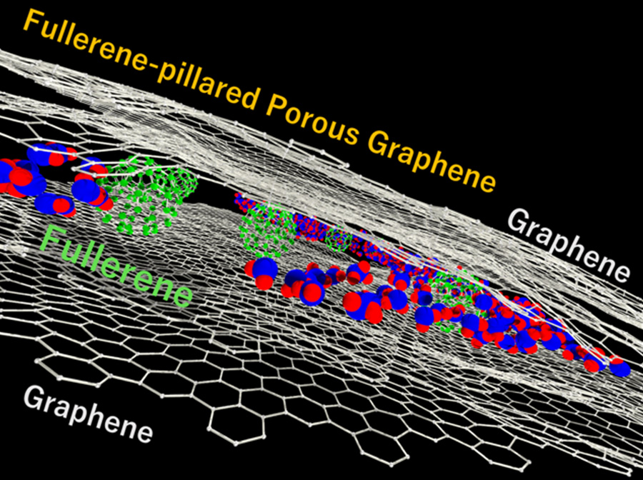
Fullerene-pillared porous graphene with high water adsorption capacity
A team of researchers from Japan has fabricated fullerene-pillared porous graphene (FPPG)—a carbon composite comprising nanocarbons—using a bottom-up approach with highly designable and controllable pore structures.
Superlubricity coating could reduce economic losses from friction, wear
Scientists at the Department of Energy’s Oak Ridge National Laboratory have invented a coating that could dramatically reduce friction in common load-bearing systems with moving parts, from vehicle drive trains to wind and hydroelectric turbines.
CA2DM@NUS and CBMM develop advanced niobium-graphene batteries with unprecedented 30-year lifecycles
Batteries play a crucial role in powering many modern devices, such as mobile phones, pacemakers, and electric vehicles. Yet, traditional lithium-ion batteries pose limitations such as safety risks, short life cycles, and long charging times. The pioneer niobium-graphene batteries developed by the Centre for Advanced 2D Materials (CA2DM) at the National University of Singapore (NUS), an innovator in the research of graphene and other 2-dimensional (2D) materials, and CBMM, the global leader in niobium products and technology, will address all these problems. The batteries are being tested at the new CBMM-CA2DM Advanced Battery Laboratory which was launched today by NUS and CBMM and established with a joint investment of USD3.8 million (S$5 million) over three years, supported by the National Research Foundation, Singapore.
UC Irvine physicists discover first transformable nano-scale electronic devices
The nano-scale electronic parts in devices like smartphones are solid, static objects that once designed and built cannot transform into anything else. But University of California, Irvine physicists have reported the discovery of nano-scale devices that can transform into many different shapes and sizes even though they exist in solid states.
Health risk of graphene residues investigated
Empa researchers have studied residues from the incineration of graphene-containing plastics. Conclusion of the study: Burned composite materials containing graphene nanoparticles can be considered harmless in case of acute exposure.
At the Edge of Graphene-Based Electronics
Researchers at the Georgia Institute of Technology have developed a new graphene-based nanoelectronics platform that could be the key to finding a successor to silicon. The team may have also discovered a new quasiparticle. Their discovery could lead to manufacturing smaller, faster, more efficient, and more sustainable computer chips, and has potential implications for quantum and high-performance computing.
Zhongwei Dai: Exploring the Strange Quantum World of 2D Materials
Zhongwei Dai, a researcher in the Interface Science and Catalysis Group of the Center for Functional Nanomaterials, probes the properties of atomically thin materials to identify promising candidates for quantum information science applications
Science snapshots from Berkeley Lab
New Berkeley Lab breakthroughs: engineering chemical-producing microbes; watching enzyme reactions in real time; capturing the first image of ‘electron ice’; revealing how skyrmions really move
One scientist’s trash is another’s treasure:
While making materials samples to pursue their own research goals, scientists at the U.S. Department of Energy’s Ames Laboratory discovered that an unwanted byproduct of their experiments was an extremely high-quality and difficult-to-obtain substance sought after by scientists researching layered materials.
Layered Graphene with a Twist Displays Unique Quantum Confinement in 2-D
Bilayer graphene with one of the two layers twisted displayed unique resonant electronic behavior. Understanding how electrons move in such 2-D materials could shed light on how to manipulate them for quantum computing and communication.
Unlocking radiation-free quantum technology with graphene
New research shows how it is possible to create heavy fermions with cheap, non-radioactive materials. To do this, the researchers used graphene.
‘Wonder material’ can be used to detect COVID-19 quickly, accurately
Researchers at the University of Illinois Chicago have successfully used graphene — one of the strongest, thinnest known materials — to detect the SARS-CoV-2 virus in laboratory experiments.
Engineers developing COVID-19 tests for mass production, mass distribution
Iowa State engineers are using their expertise in graphene-based biosensors to develop quick, inexpensive and sensitive saliva tests for the virus that causes COVID-19. Federal agencies are supporting the research with the goal of producing tests that can be easily mass produced and widely distributed.
Story tips: Quantum building blocks, high-pressure diamonds, wildfire ecology, quick cooling tooling and printing on the fly
ORNL story tips: Quantum building blocks, high-pressure diamonds, wildfire ecology, quick cooling tooling and printing on the fly
Quantum tunneling in graphene advances the age of terahertz wireless communications
Scientists from MIPT, Moscow Pedagogical State University and the University of Manchester have created a highly sensitive terahertz detector based on the effect of quantum-mechanical tunneling in graphene. The sensitivity of the device is already superior to commercially available analogs based on semiconductors and superconductors, which opens up prospects for applications of the graphene detector in wireless communications, security systems, radio astronomy, and medical diagnostics. The research results are published in a high-rank journal Nature Communications.
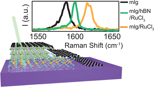
New way to control electrical charge in 2D materials: Put a flake on it
Physicists at Washington University in St. Louis have discovered how to locally add electrical charge to an atomically thin graphene device by layering flakes of another thin material, alpha-RuCl3, on top of it. A paper published with scientists at Boston College describes the charge transfer process in detail. Gaining control of the flow of electrical current through atomically thin materials is important to potential future applications in photovoltaics or computing.
New Platform Generates Hybrid Light-Matter Excitations in Highly Charged Graphene
Columbia University researchers report that they have achieved plasmonically active graphene with record-high charge density without an external gate. They accomplished this by exploiting novel interlayer charge transfer with a two-dimensional electron-acceptor known as -RuCl3. “This work allows us to use graphene as a plasmonic material without metal gates or voltage sources, making it possible to create stand-alone graphene plasmonic structures for the first time,” said Mechanical Engineering Prof. James Hone.
No losses: Scientists stuff graphene with light
Physicists from MIPT and Vladimir State University, Russia, have achieved a nearly 90% efficiency converting light energy into surface waves on graphene. They relied on a laser-like energy conversion scheme and collective resonances.
Charges Cascading Along a Molecular Chain
Removing one charged molecule from a one-dimensional array causes the others to alternately turn ‘on’ or ‘off,’ paving the way for information transfer in tiny circuits
Graphene-based memristors show promise for brain-based computing
As progress in traditional computing slows, new forms of computing are coming to the forefront. At Penn State, a team of engineers is attempting to pioneer a type of computing that mimics the efficiency of the brain’s neural networks while exploiting the brain’s analog nature.

Los Alamos scientists find a way to quickly test rust on graphene-protected cars, planes, ships
Trace amounts of graphene could create a decades-long protective barrier against oxygen corrosion for cars, aircrafts, and ships–but evaluating its effectiveness has been a challenge, until now.
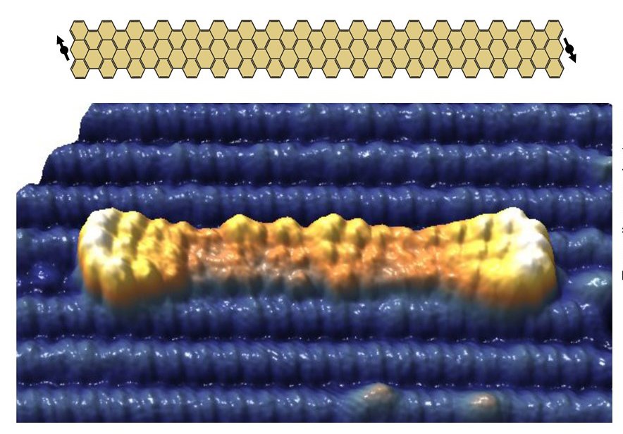
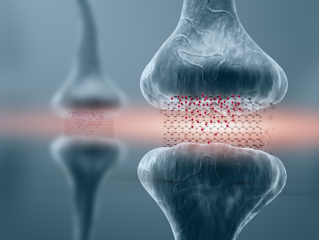
On-surface synthesis of graphene nanoribbons could advance quantum devices
An international multi-institution team of scientists has synthesized graphene nanoribbons – ultrathin strips of carbon atoms – on a titanium dioxide surface using an atomically precise method that removes a barrier for custom-designed carbon nanostructures required for quantum information sciences.
Automating 2-D Material Exfoliation with Suji Park
Park, a staff researcher at Brookhaven Lab’s Center for Functional Nanomaterials, is designing and building an automated system to generate high-quality ultrathin “flakes,” which can be stacked into layered structures that are essentially new materials.
All together now: Experiments with twisted 2D materials catch electrons behaving collectively
A team led by the University of Washington reports that carefully constructed stacks of graphene — a 2D form of carbon — can exhibit highly correlated electron properties. The team also found evidence that this type of collective behavior likely relates to the emergence of exotic magnetic states.
Graphene expert comments on the creation of an extremely tiny magnetic field detector
“The research group from the University of Basel has recently created an ultracompact superconducting quantum interference device — aka SQUID, where the record miniaturization is achieved by using next-generation materials: bilayer graphene-based van der Waals heterostructures. SQUIDs usually consist of two…
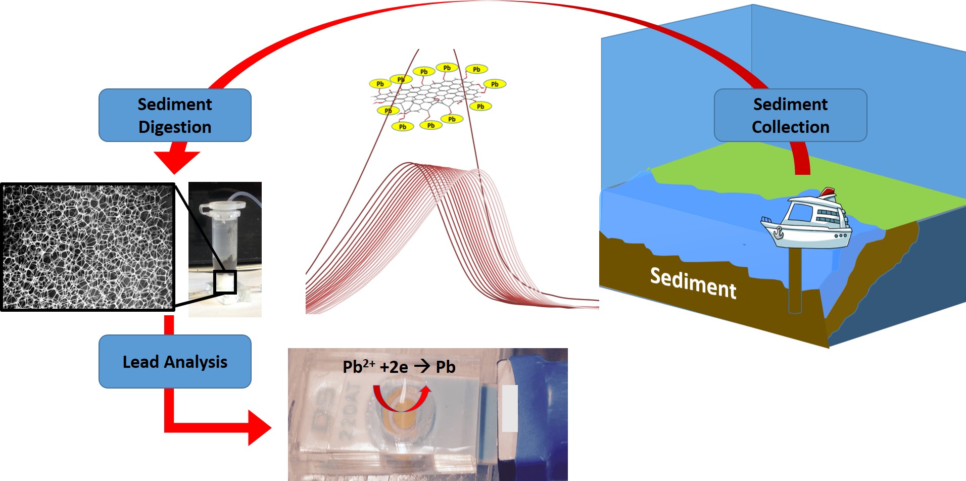
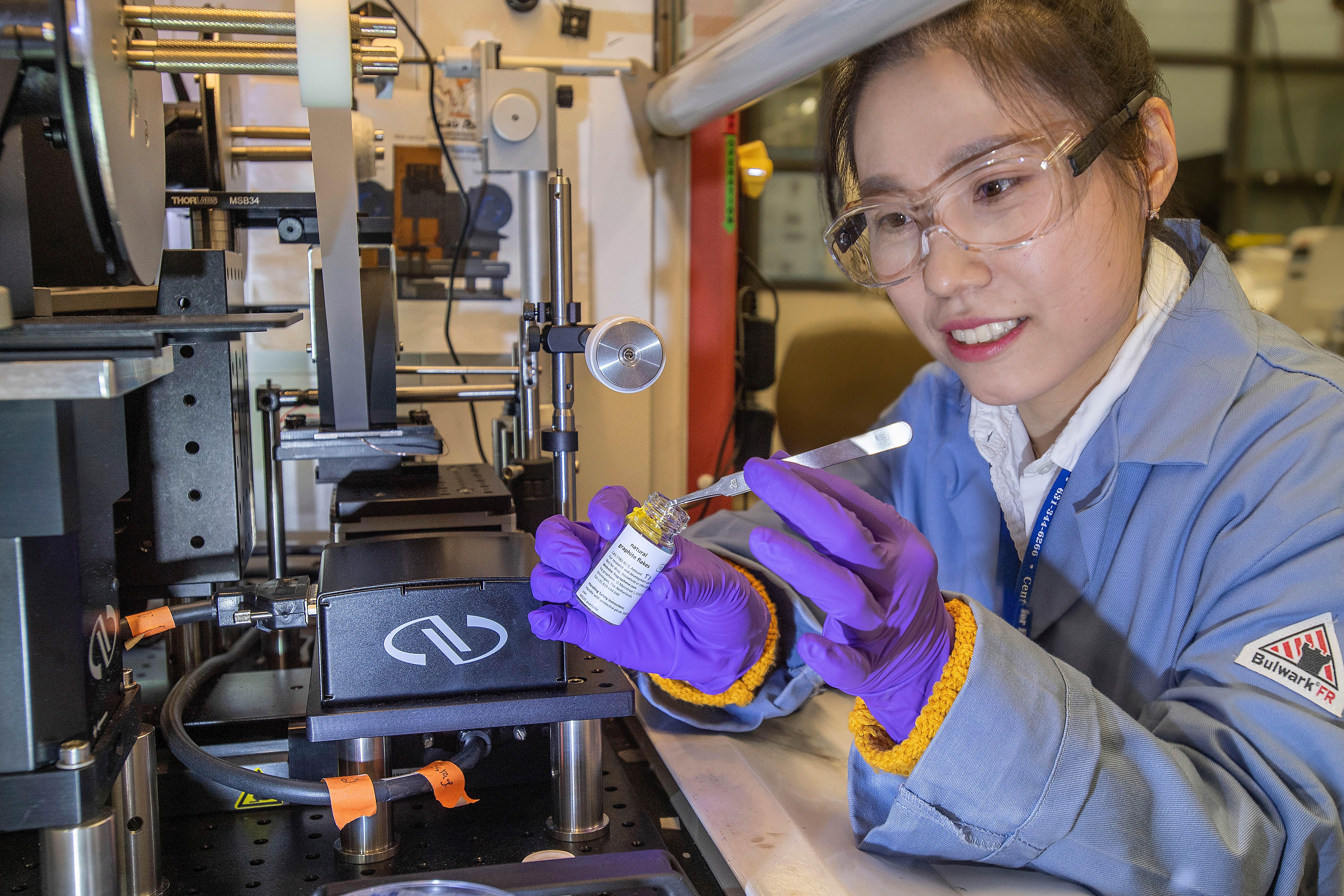
New Device Can Measure Toxic Lead Within Minutes
Rutgers researchers have created a miniature device for measuring trace levels of toxic lead in sediments at the bottom of harbors, rivers and other waterways within minutes – far faster than currently available laboratory-based tests, which take days. The affordable lab-on-a-chip device could also allow municipalities, water companies, universities, K-12 schools, daycares and homeowners to easily and swiftly test their water supplies. The research is published in the IEEE Sensors Journal.
Henriksen lands CAREER grant to chase electron effects
Erik Henriksen, assistant professor of physics in Arts & Sciences at Washington University in St. Louis, has been awarded a prestigious Faculty Early Career Development (CAREER) Award by the National Science Foundation. His grant, expected to total $850,000 over the next five years, is for research that explores many-particle interactions in graphene and other single-atom-thick materials.

Quantum Materials Quest Could Benefit From Graphene That Buckles
Graphene, an extremely thin two-dimensional layer of the graphite used in pencils, buckles when cooled while attached to a flat surface, resulting in beautiful pucker patterns that could benefit the search for novel quantum materials and superconductors, according to Rutgers-led research in the journal Nature. Quantum materials host strongly interacting electrons with special properties, such as entangled trajectories, that could provide building blocks for super-fast quantum computers. They also can become superconductors that could slash energy consumption by making power transmission and electronic devices more efficient.
Physicists Find Misaligned Carbon Sheets Yield Unparalleled Properties
A material composed of two one-atom-thick layers of carbon has grabbed the attention of physicists worldwide for its intriguing — and potentially exploitable — conductive properties.
Researchers print, tune graphene sensors to monitor food freshness, safety
Researchers are using high-resolution printing technology and the unique properties of graphene to make low-cost biosensors to monitor food safety and livestock health.
With a ‘catch-and-release’ process, researchers advance graphene electronics
A team of researchers has found a versatile method for the construction of high-quality vdW heterostructures using a dual-function polymeric film with a thickness of below five nanometers to promote the exfoliation of monolayer graphene.
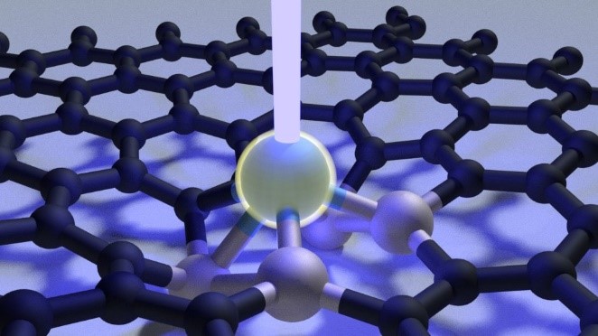
Joined nano-triangles pave the way to magnetic carbon materials
Graphene triangles with an edge length of only a few atoms behave like peculiar quantum magnets. When two of these nano-triangles are joined, a “quantum entanglement” of their magnetic moments takes place: the structure becomes antiferromagnetic. This could be a breakthrough for future magnetic materials, and another step towards spintronics. An international group led by Empa researchers recently published the results in the journal “Angewandte Chemie”.
Preventing metal pipe corrosion
A thin, single layer of graphene material only 1 atom thick may reduce metal pipe corrosion rates as much as 100 times. These new crystalline 2D materials could mean big savings to industries.
UIC chemical engineers get ‘muddy’ to develop renewable fuel cell
University of Illinois at Chicago engineers digging for efficient ways to harness sustainable power found a surprising fuel source — mud and a common bacterium often found in it.
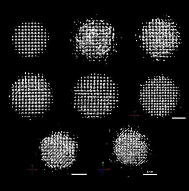
Science Snapshots from Berkeley Lab: 3D nanoparticles and magnetic spin
Researchers at Berkeley Lab have captured 3D images of nanoparticles in liquid with atomic precision, and developed an ultrathin electrical switch that could further miniaturize computing devices and personal electronics without loss of performance.
Story Tips: Molding matter atom by atom and seeing inside uranium particles
Story Tips: Molding matter atom by atom and seeing inside uranium particles, from the Department of Energy’s Oak Ridge National Laboratory
Two-Dimensional Metals Open Pathways to New Science
A new, atomically-thin materials platform developed by Penn State researchers in conjunction with Lawrence Berkeley National Lab and Oak Ridge National Lab will open a wide range of new applications in biomolecular sensing, quantum phenomena, catalysis and nonlinear optics.
A Talented 2D Material Gets a New Gig
Berkeley Lab scientists tap into graphene’s hidden talent as an electrically tunable superconductor, insulator, and magnetic device for the advancement of quantum information science

Columbia Researchers Develop New Method to Isolate Atomic Sheets and Create New Materials
Columbia researchers have invented a new method—using ultraflat gold films—to disassemble vdW single crystals layer by layer into monolayers with near-unity yield and with dimensions limited only by bulk crystal sizes. The monolayers have the same high quality as those created by conventional “Scotch tape” exfoliation, but are roughly a million times larger. They can be assembled into macroscopic artificial structures, with properties not easily created in conventionally grown bulk crystals.
When Electrons Follow New Interaction Rules, Superconductivity Ensues
Researchers used a scanning tunneling microscope to “see” the electron interactions and pairings at the heart of twisted bilayer graphene’s novel properties.
Breaking (and Restoring) Graphene’s Symmetry in a Twistable Electronics Device
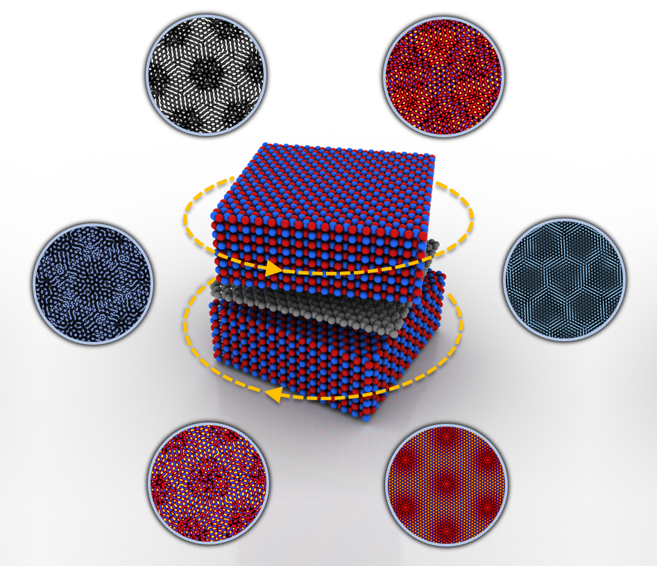
A recent Columbia Engineering study demonstrates a new way to tune the properties of 2D materials simply by adjusting the twist angle between them. The researchers built devices consisting of monolayer graphene encapsulated between two crystals of boron nitride and, by adjusting the relative twist angle between the layers, they were able to create multiple moiré pattern—“the first time anyone has seen the full rotational dependence of coexisting moiré superlattices in one device.”

A four-way switch promises greater tunability of layered materials
A team from Oak Ridge National Laboratory and Vanderbilt University made the first experimental observation of a material phase that had been predicted but never seen.