A new $1 million in funding will help Binghamton University, State University of New York provide job training for more than 100 students a year in the growing advanced chip manufacturing industry.
Tag: Semiconductors
Electrons screen against conductivity-killer in organic semiconductors
Scientists uncover the physics driving dopant and polymer interactions that boost conductivity in organic materials.
How robots can help find the solar energy of the future
Solar energy is one of the most promising ways to power the world of the future. However, creating more efficient solar cells requires finding new and better materials.
Accelerating Sustainable Semiconductors With ‘Multielement Ink’
Scientists have demonstrated “multielement ink” – the first “high-entropy” semiconductor that can be processed at low-temperature or room temperature. The new material could enable cost-effective and energy-efficient semiconductor manufacturing.
Scientists uncovered mystery of important material for semiconductors at the surface
A team of scientists with Oak Ridge National Laboratory has investigated the behavior of hafnium oxide, or hafnia, because of its potential for use in novel semiconductor applications.
Bigger and better quantum computers possible with new ion trap, dubbed the Enchilada
Sandia National Laboratories has produced its first lot of a new world-class ion trap, a central component for certain quantum computers.

University of Illinois Professor Rakesh Kumar – expert on semiconductors, issues at the intersection of technology, policy, and society
Rakesh Kumar is professor in the Electrical and Computer Engineering Department at the University of Illinois Urbana-Champaign with research and teaching interests in computer architecture. Kumar can serve as a source for articles at the intersection of technology, policy, and…
Xiaodong Xu: Then and Now / 2012 Early Career Award Winner
University of Washington professor Xiaodong Xu studies the properties of single atomic layer semiconductors, looking for new materials and new ways to control electrical conductivity.
New material could hold key to reducing energy consumption in computers and electronics
A University of Minnesota Twin Cities team has, for the first time, synthesized a thin film of a unique topological semimetal material that has the potential to generate more computing power and memory storage while using significantly less energy.
New superconducting diode could improve performance of quantum computers and artificial intelligence
A University of Minnesota Twin Cities-led team has developed a more energy-efficient, tunable superconducting diode—a promising component for future electronic devices—that could help scale up quantum computers for industry and improve artificial intelligence systems.

Kirstin Alberi: Then and Now / 2012 Early Career Award Winner
Kirstin Alberi is Director of the Materials Science Center at the National Renewable Energy Laboratory. Her research into semiconductor materials shows that scientists can use light as a tool while depositing materials as a vapor and controlling the substrate’s temperature.
Answering Big Questions with Thin Oxide Films
Thin oxide films play an important role in electronics and energy storage. Researchers in PNNL’s film growth laboratory create, explore, and improve new thin oxide films.
Researchers create breakthrough spintronics manufacturing process that could revolutionize the electronics industry
University of Minnesota Twin Cities researchers, along with staff at the National Institute of Standards and Technology (NIST), have developed a breakthrough process for making spintronic devices that has the potential to create semiconductors chips with unmatched energy efficiency and storage for use in computers, smartphones, and many other electronics.
National Science Foundation awards $90.8M to Arizona State University to advance X-ray science
The National Science Foundation today announced $90.8 million in funding to Arizona State University — the largest NSF research award in the university’s history — to advance groundbreaking research in X-ray science.
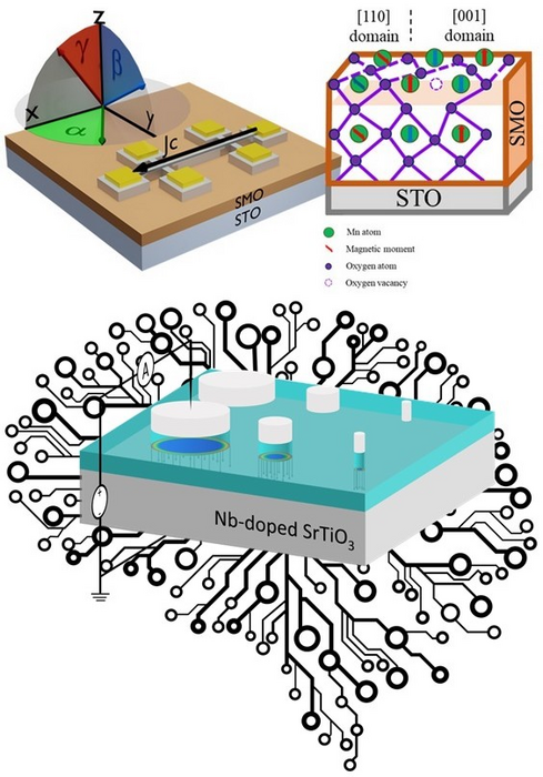
Complex oxides could power the computers of the future
As the evolution of standard microchips is coming to an end, scientists are looking for a revolution. The big challenges are to design chips that are more energy efficient and to design devices that combine memory and logic (memristors).
New Technology Turns Smartphones into RFID Readers, Saving Costs and Reducing Waste
Imagine you can open your fridge, open an app on your phone and immediately know which items are expiring within a few days. This is one of the applications that a new technology developed by engineers at the University of California San Diego would enable.
First-of-its-kind instrument officially ushers in new era of X-ray science
Arizona State University has officially begun a new chapter in X-ray science with a newly commissioned, first-of-its-kind instrument that will help scientists see deeper into matter and living things. The device, called the compact X-ray light source (CXLS), marked a major milestone in its operations as ASU scientists generated its first X-rays on the night of Feb. 2.
Cornell to lead new semiconductor research center
Cornell is leading a new $34 million research center that will accelerate the creation of energy-efficient semiconductor materials and technologies, and develop revolutionary new approaches for microelectronics systems.
Self-powered, printable smart sensors created from emerging semiconductors could mean cheaper, greener Internet of Things
Creating smart sensors to embed in our everyday objects and environments for the Internet of Things (IoT) would vastly improve daily life—but requires trillions of such small devices.
At the Edge of Graphene-Based Electronics
Researchers at the Georgia Institute of Technology have developed a new graphene-based nanoelectronics platform that could be the key to finding a successor to silicon. The team may have also discovered a new quasiparticle. Their discovery could lead to manufacturing smaller, faster, more efficient, and more sustainable computer chips, and has potential implications for quantum and high-performance computing.
Laser controls ultra-fast liquid switch
All the operations of computers and smartphones are based on circuits.
Growing pure nanotubes is a stretch, but possible
Like a giraffe stretching for leaves on a tall tree, making carbon nanotubes reach for food as they grow may lead to a long-sought breakthrough.
Senators, industry leaders discuss the meaning of CHIPS Act to national economy and security
Two panel discussions overviewed the importance of the new $52-billion CHIPS and Science Act as a catalyst for improving American research, manufacturing, workforce development and national security related to semiconductors. The event was hosted by Arizona State University and the Washington Business Journal on Sept. 22 in Washington, D.C.
A new neuromorphic chip for AI on the edge, at a small fraction of the energy and size of today’s compute platforms
An international team of researchers has designed and built a chip that runs computations directly in memory and can run a wide variety of AI applications–all at a fraction of the energy consumed by computing platforms for general-purpose AI computing. The NeuRRAM neuromorphic chip brings AI a step closer to running on a broad range of edge devices, disconnected from the cloud, where they can perform sophisticated cognitive tasks anywhere and anytime without relying on a network connection to a centralized server.
The Best Semiconductor of Them All?
Silicon is one of the most abundant elements on Earth, and in its pure form the material has become the foundation of much of modern technology, from solar cells to computer chips. But silicon’s properties as a semiconductor are far from ideal.
Researchers solve mystery surrounding dielectric properties of unique metal oxide
A University of Minnesota Twin Cities-led research team has solved a longstanding mystery surrounding strontium titanate, a metal oxide semiconductor, providing insight for future research on the material and its applications to electronic devices and data storage.
‘Fruitcake’ Structure Observed in Organic Polymers
Researchers have analysed the properties of an organic polymer with potential applications in flexible electronics and uncovered variations in hardness at the nanoscale, the first time such a fine structure has been observed in this type of material.
Study uncovers how structural changes affect the superconducting properties of a metal oxide
A team led by University of Minnesota Twin Cities researchers has discovered how subtle structural changes in strontium titanate, a metal oxide semiconductor, can alter the material’s electrical resistance and affect its superconducting properties. The research can help guide future experiments and materials design related to superconductivity and the creation of more efficient semiconductors for various electronic device applications.
Metal-Halide Perovskite Semiconductors Can Compete with Silicon Counterparts for Solar Cells, LEDs
Common semiconductor materials for solar cells, such as silicon, must be grown via an expensive process to avoid defects within their crystal structure that affect functionality. But metal-halide perovskite semiconductors are emerging as a cheaper, alternative material class, with excellent and tunable functionality as well as easy processability.
Science snapshots from Berkeley Lab
New Berkeley Lab breakthroughs: engineering chemical-producing microbes; watching enzyme reactions in real time; capturing the first image of ‘electron ice’; revealing how skyrmions really move
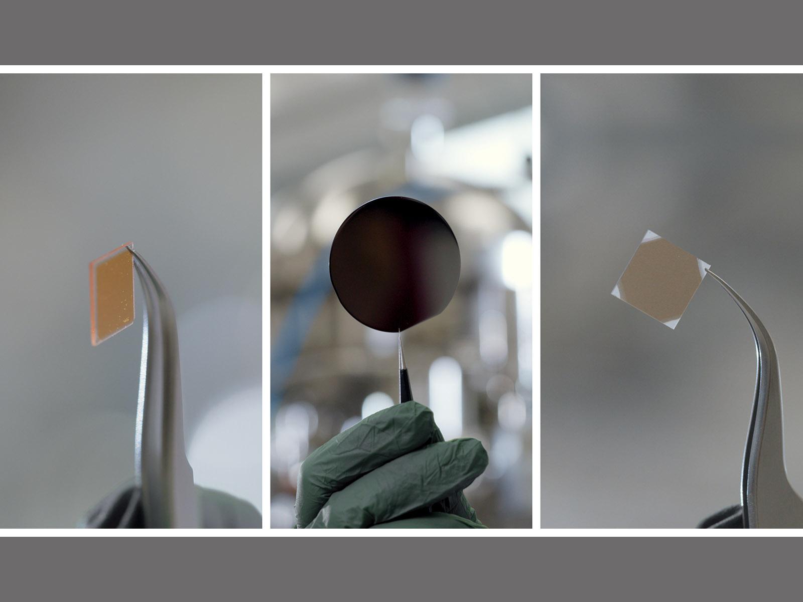
A simple way to get complex semiconductors to assemble themselves
A new way to make complex, layered semiconductors is like making rock candy: They assemble themselves from chemicals in water. The method will aid design and large-scale production of these materials.
LLNL, other Bay Area labs to host webinar about business partnerships, the future of semiconductors
Lawrence Livermore National Laboratory and its three partner national labs in the Bay Area Lab Innovation Networking Center (LINC) will offer a webinar about the future of semiconductors and advanced materials on Wednesday, Aug. 25.
MITRE Engenuity Forms Alliance to Define Strategy for U.S. Investment in Semiconductor Innovation
MITRE Engenuity has established a semiconductor alliance to help define strategy for U.S. investment in this critical area.
As EVs take off, semiconductor demand to rise amidst chip shortage
President Biden is meeting with lawmakers on Wednesday to discuss a critical global shortage of semiconductors — computer chips used in cars, consumer electronics and weapons systems. The administration is also expected to order a 100-day review of U.S. supply…
Dynamic Duos: How Particles Attach
Researchers have established a quantitative understanding of how nano-sized dipole particles assemble and crystalize. The driving force is the weak long-range attractive interaction between the dipoles that aligns the crystal faces of the particles prior to their collision. Stronger attractive forces then drive the final jump to connect the particles.
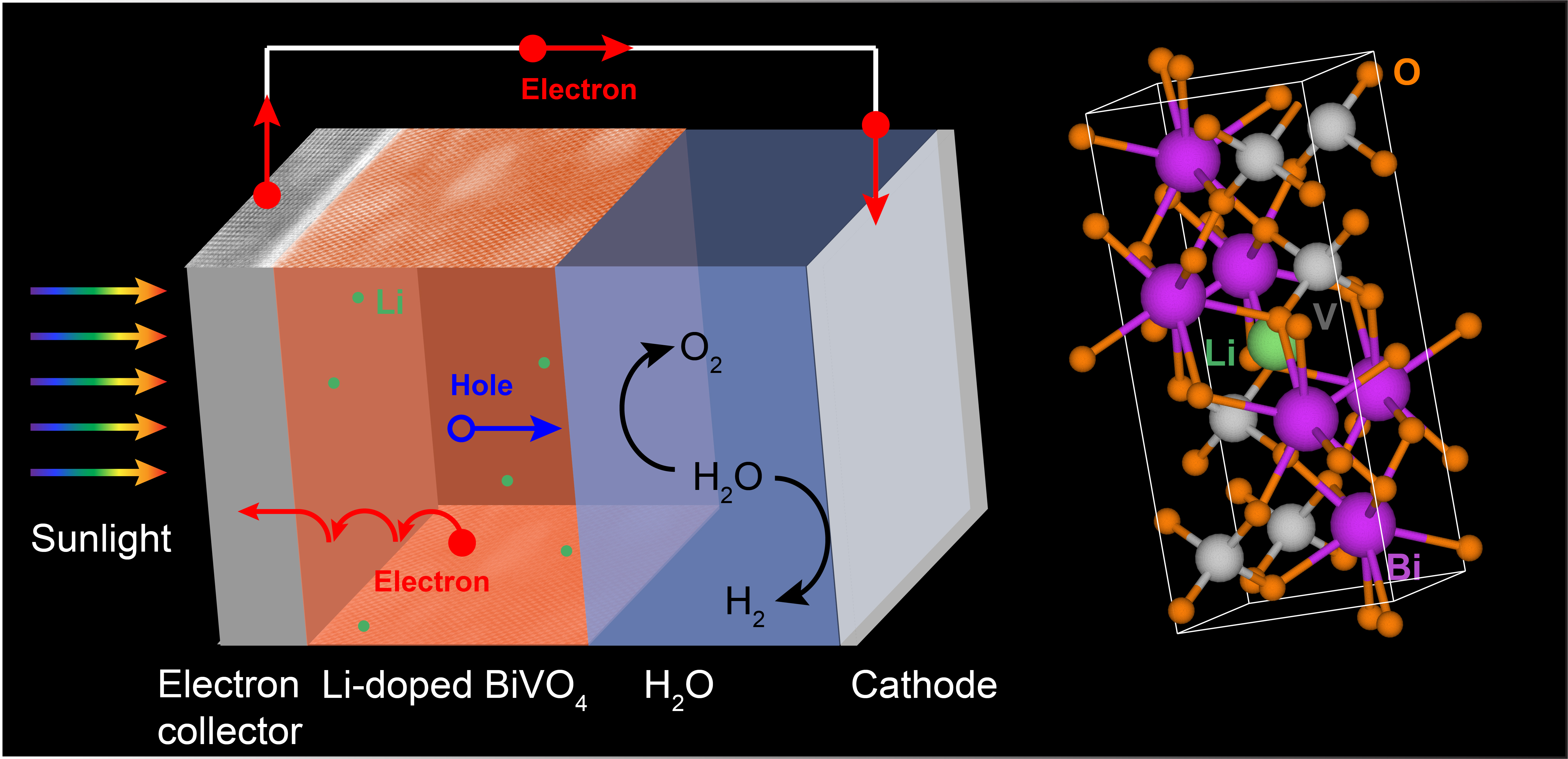
Driving Water Splitting to Create Chemical Fuels
Scientists improved the performance of bismuth vanadate, an electrode material for converting solar energy to hydrogen—an energy-dense and clean-burning fuel.
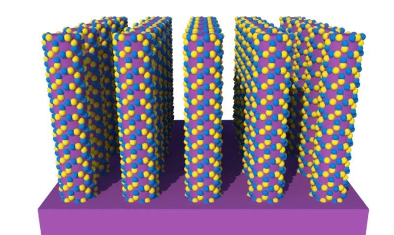
Decorating Semiconductors at the Atomic Scale
Combining two different semiconductors can create new properties. The way these combinations work depends on how the semiconductors are arranged and contact one another. Researchers have developed a new way to grow semiconductor crystals about 100,000 times smaller than the width of a human hair. This new synthesis method independently controls the arrangements and sizes of the crystals.
Breaking the Power & Speed Limit of Lasers
SUMMARYResearchers at the George Washington University have developed a new design of vertical-cavity surface-emitting laser (VCSEL) that demonstrates record-fast temporal bandwidth. This was possible by combining multiple transverse coupled cavities, which enhances optical feedback of the laser. VCSELs have emerged…
Berkeley Lab Part of Multi-Institutional Team Awarded $60M for Solar Fuels Research
The Department of Energy has awarded $60 million to a new solar fuels initiative – called the Liquid Sunlight Alliance (LiSA) – led by Caltech in close partnership with Berkeley Lab. LiSA will build on the foundational work of the Joint Center for Artificial Photosynthesis (JCAP).
Scientists Dive Deep Into Hidden World of Quantum States
A research team led by the Department of Energy’s Lawrence Berkeley National Laboratory (Berkeley Lab) has developed a technique that could lead to new electronic materials that surpass the limitations imposed by Moore’s Law.

Laser allows solid-state refrigeration of a semiconductor material
A team from the University of Washington used an infrared laser to cool a solid semiconductor by at least 20 degrees C, or 36 F, below room temperature, as they report in a paper published June 23 in Nature Communications.
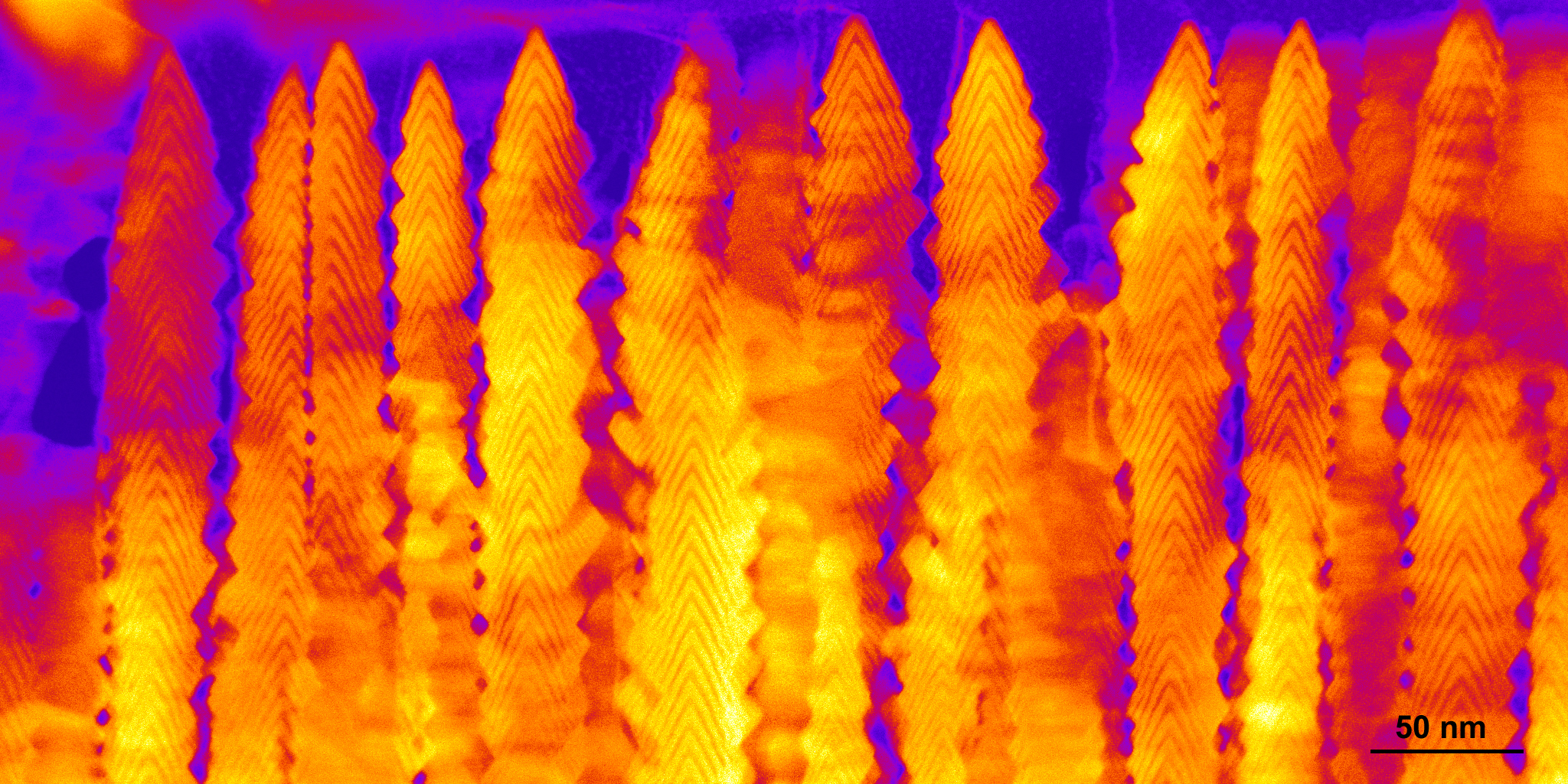
Crystalline ‘nanobrush’ clears way to advanced energy and information tech
A team led by Oak Ridge National Laboratory synthesized a “nanobrush” structure with high surface area and discovered how its unique architecture drives ions across interfaces to transport energy or information.

Linking Properties to Defects in 2D Materials
Scientists measured the atomic and electronic structure of a two-dimensional semiconductor to understand defects in the crystal structure. The measurements were made at the same time and at the same location, and the quantum orbitals associated with the defects were visualized using an ultra-sharp probe made from a single carbon monoxide molecule.
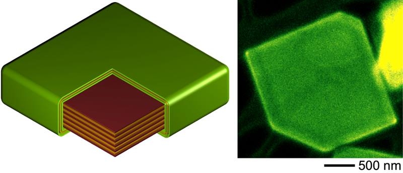
Wrapped, Layered Semiconductors Catch the Light
Heterostructures are semiconductors that have special optical and electronic properties. Researchers discovered a new way to make heterostructures that consist of a core of tin sulfide crystals wrapped in a tin disulfide shell, a structure with excellent light absorption and energy transfer properties.
How JCAP Is Making Solar Fuels Shine
As we look back at a decade of discovery, we highlight 10 achievements by scientists at Berkeley Lab and the Joint Center for Artificial Photosynthesis that bring us closer to a solar fuels future.