The organization, which consists of state-wide partnerships between institutions of higher education, governmental bodies, and members of private industry, will help develop Utah’s semiconductor workforce and increase its access to key technological infrastructure.
Tag: Semiconductor
Tough memory device aims for space missions
Among the many hazards encountered by space probes, exposure to radiation and huge temperature swings pose particular challenges for their electronic circuits. Now KAUST researchers have invented the first ever flash memory device made from gallium oxide, a material that can withstand these harsh conditions far better than conventional electronics.

GridTrust Helps Protect the Nation’s Electric Utilities from Cyber Threats
A new cybersecurity technology that relies on the unique digital fingerprint of individual semiconductor chips could help protect the equipment of electrical utilities from malicious attacks that exploit software updates on devices controlling the critical infrastructure.
Forging a dream material with semiconductor quantum dots
Researchers from the RIKEN Center for Emergent Matter Science and collaborators have succeeded in creating a “superlattice” of semiconductor quantum dots that can behave like a metal, potentially imparting exciting new properties to this popular class of materials.
Electronic bridge allows rapid energy sharing between semiconductors
As semiconductor devices become ever smaller, researchers are exploring two-dimensional materials for potential applications in transistors and optoelectronics. Controlling the flow of electricity and heat through these materials is key to their functionality, but first we need to understand the details of those behaviors at atomic scales. Now, researchers have discovered that electrons play a surprising role in how energy is transferred between layers of 2D semiconductor materials tungsten diselenide and tungsten disulfide.
Teaching photonic chips to learn
A multi-institution research team has developed an optical chip that can train machine learning hardware.
GW faculty experts are available to discuss congressional semiconductor legislation from political and scientific perspectives.
After months of negotiations between both parties and both chambers on Capitol Hill, the Senate appears poised to hold a vote on more than $50 billion in incentives for domestic semiconductor production. Senate leaders hope this measure can bridge the…
NUS researchers develop brain-inspired memory device that can revolutionise semiconductor design
Many electronic devices today are dependent on semiconductor logic circuits based on switches hard-wired to perform predefined logic functions. Physicists from the National University of Singapore (NUS), together with an international team of researchers, have developed a novel molecular memristor, or an electronic memory device, that has exceptional memory reconfigurability.
LED Material Shines Under Strain
A team led by researchers at Lawrence Berkeley National Laboratory (Berkeley Lab) and UC Berkeley has demonstrated an approach for achieving LEDs with near 100% light-emission efficiency at all brightness levels.
MITRE Engenuity Forms Alliance to Define Strategy for U.S. Investment in Semiconductor Innovation
MITRE Engenuity has established a semiconductor alliance to help define strategy for U.S. investment in this critical area.
This hydrogen fuel machine could be the ultimate guide to self improvement
Scientists at Berkeley have uncovered an extraordinary self-improving property that transforms an ordinary semiconductor into a highly efficient and stable artificial photosynthesis device
Breaking the Power & Speed Limit of Lasers
SUMMARYResearchers at the George Washington University have developed a new design of vertical-cavity surface-emitting laser (VCSEL) that demonstrates record-fast temporal bandwidth. This was possible by combining multiple transverse coupled cavities, which enhances optical feedback of the laser. VCSELs have emerged…
Story Tips: Remote population counting, slowing corrosion and turning down the heat
ORNL story tips: Remote population counting, slowing corrosion and turning down the heat
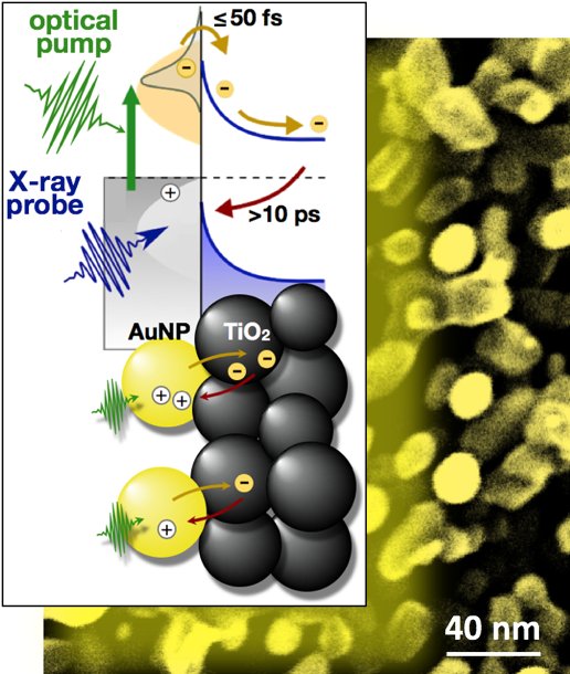
Scientists Capture Candid Snapshots of Electrons Harvesting Light at the Atomic Scale
A team of scientists led by Berkeley Lab has gained important new insight into electrons’ role in the harvesting of light in artificial photosynthesis systems.
New fabrication method brings single-crystal perovskite devices closer to viability
Nanoengineers at UC San Diego developed a new method to fabricate perovskites as single-crystal thin films, which are more efficient for use in solar cells and optical devices than the current state-of-the-art polycrystalline forms of the material.
Tiny Bubbles Make a Quantum Leap
Researchers at Columbia Engineering and Montana State University have found that placing sufficient strain in a 2D material creates localized states that can yield single-photon emitters. Using sophisticated optical microscopy techniques developed at Columbia over the past 3 years, the team was able to directly image these states for the first time, revealing that even at room temperature they are highly tunable and act as quantum dots, tightly confined pieces of semiconductors that emit light.

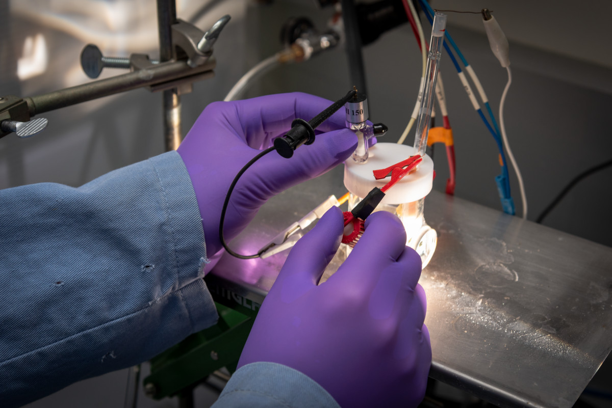
Laser allows solid-state refrigeration of a semiconductor material
A team from the University of Washington used an infrared laser to cool a solid semiconductor by at least 20 degrees C, or 36 F, below room temperature, as they report in a paper published June 23 in Nature Communications.
Emerging Wide Bandgap Semiconductor Devices Based on Silicon Carbide May Revolutionize Power Electronics
Silicon plays a central role within the semiconductor industry for microelectronic and nanoelectronic devices, and silicon wafers of high purity single-crystalline material can be obtained via a combination of liquid growth methods. In Applied Physics Reviews, researchers describe the atomic mechanisms governing extended defect kinetics in cubic silicon carbide, which has a diamondlike zincblende crystal structure that manifests stacking and anti-phase instabilities. The study pinpoints the atomistic mechanisms responsible for extended defect generation and evolution.

Columbia Researchers Develop New Method to Isolate Atomic Sheets and Create New Materials
Columbia researchers have invented a new method—using ultraflat gold films—to disassemble vdW single crystals layer by layer into monolayers with near-unity yield and with dimensions limited only by bulk crystal sizes. The monolayers have the same high quality as those created by conventional “Scotch tape” exfoliation, but are roughly a million times larger. They can be assembled into macroscopic artificial structures, with properties not easily created in conventionally grown bulk crystals.
Coronavirus multiple-times worse than SARS: Global supply-chain effect could exceed $400bn, linger up to 2 years — WashU expert
Panos Kouvelis 314-935-4604 [email protected] Please read: https://source.wustl.edu/2020/02/washu-expert-coronavirus-far-greater-threat-than-sars-to-global-supply-chain/ Please watch: https://youtu.be/ATzgs67Dnx8 Original post https://alertarticles.info

Crystal with a Twist: Researchers Grow Spiraling New Material
Scientists have created new inorganic crystals made of stacks of atomically thin sheets.
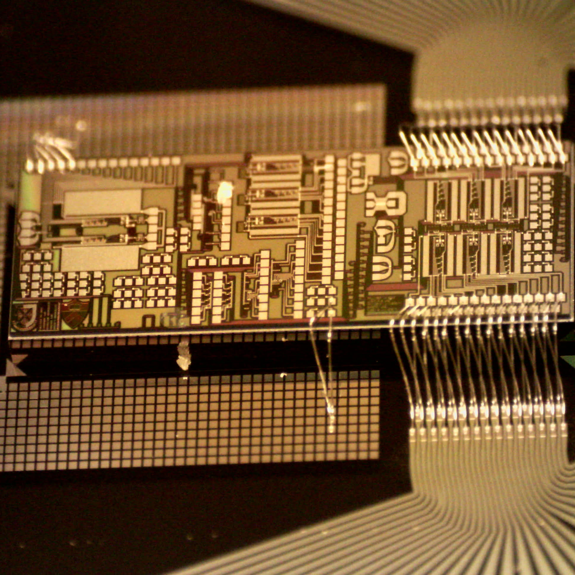
Scientists see defects in potential new semiconductor
A research team has reported seeing, for the first time, atomic scale defects that dictate the properties of a new and powerful semiconductor. The study, published earlier this month in the journal Physical Review X, shows a fundamental aspect of how the semiconductor, beta gallium oxide, controls electricity.

The Beauty of Imperfections: Linking Atomic Defects to 2D Materials’ Electronic Properties
Scientists at Berkeley Lab have revealed how atomic defects emerge in transition metal dichalcogenides, and how those defects shape the 2D material’s electronic properties. Their findings could provide a versatile yet targeted platform for designing 2D materials for quantum information science.
Gordon Bell Finalist Team Tackles Transistors with New Programming Paradigm
A team simulated a 10,000-atom 2D transistor slice on the Summit supercomputer and mapped where heat is produced in a single transistor. Using a new data-centric version of the OMEN nanodevice simulator, the team sustained the code at 85.45 petaflops and earned a Gordon Bell Prize finalist nomination.