Researchers at the U.S. Department of Energy’s Princeton Plasma Physics Laboratory are applying their expertise in physics, chemistry and computer modeling to create the next generation of computer chips, aiming for processes and materials that will produce chips with smaller features.
Tag: Microelectronics
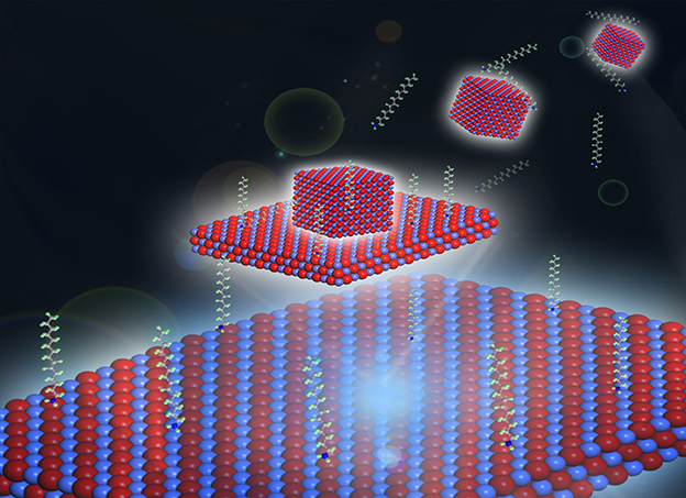
Groundbreaking Microcapacitors Could Power Chips of the Future
Berkeley Lab scientists have achieved record-high energy and power densities in microcapacitors made with engineered thin films, using materials and fabrication techniques already widespread in chip manufacturing.
New Technique Lets Scientists Create Resistance-Free Electron Channels
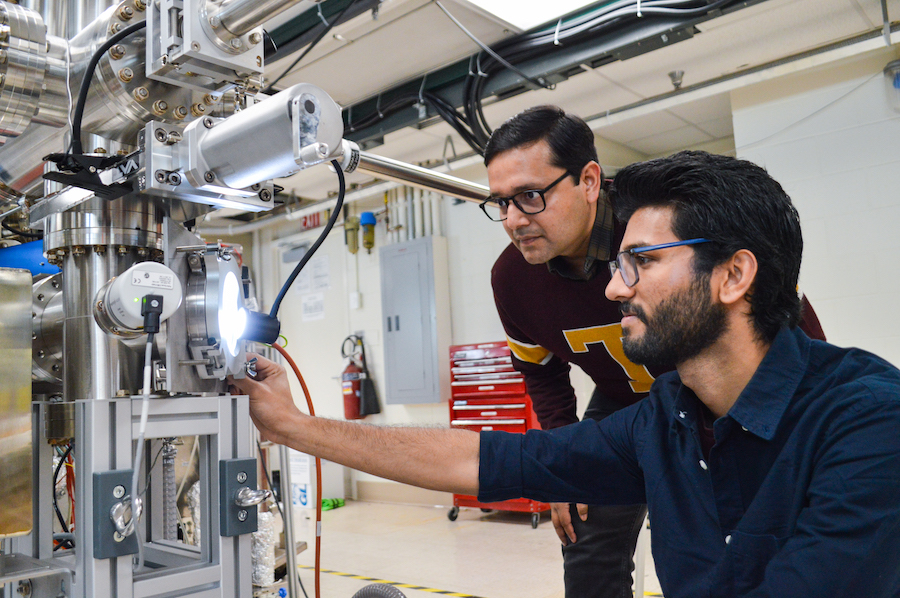
Researchers have taken the first atomic-resolution images and demonstrated electrical control of a chiral interface state – an exotic quantum phenomenon that could help researchers advance quantum computing and energy-efficient electronics.
Vlasov and Bashir groups develop nanoscale device for brain chemistry analysis
The device, developed by researchers at the University of Illinois Urbana-Champaign, is silicon-based and takes advantage of techniques developed for microelectronics manufacturing.
How Scientists Are Accelerating Next-Gen Microelectronics
In a new Q&A, microelectronics expert and CHiPPS Director Ricardo Ruiz shares his perspective on keeping pace with Moore’s Law in the decades to come through a revolutionary technique called extreme ultraviolet lithography.
Bigger and better quantum computers possible with new ion trap, dubbed the Enchilada
Sandia National Laboratories has produced its first lot of a new world-class ion trap, a central component for certain quantum computers.
DOE Announces $72 Million For Small Business Research and Development Grants
The U.S. Department of Energy (DOE) today announced $72 million in funding for small businesses to pursue scientific, clean energy, and climate research, development, and demonstration projects. The funding will support 296 projects across 44 states and addresses multiple topic areas, such as renewable energy, nuclear energy, cybersecurity, advanced materials and manufacturing, microelectronics, and artificial intelligence. Today’s announcement underscores the Biden-Harris Administration’s deep commitment to advancing innovative climate solutions and strengthening America’s global scientific leadership, which are critical to achieving the President’s goal of a carbon-free grid by 2035 and net-zero emissions by 2050.
Stretching metals at the atomic level allows researchers to create important materials for quantum, electronic, and spintronic applications
A University of Minnesota Twin Cities-led team has developed a first-of-its-kind breakthrough method that makes it easier to create high-quality metal oxide films that are important for various next generation applications such as quantum computing and microelectronics.

DARPA projects designing microelectronics platforms for the future
The recipient of grants from the U.S. Department of Defense Advanced Research Projects Agency, or DARPA, totaling $22.4 million, ASU Professor Daniel Bliss is now working on two advanced computing projects, both of which are producing reimagined “chips,” or microprocessors, that are the foundation for most of today’s electronics — from supercomputers to smart devices to the technology that makes autonomous vehicles self-driving.
At the Edge of Graphene-Based Electronics
Researchers at the Georgia Institute of Technology have developed a new graphene-based nanoelectronics platform that could be the key to finding a successor to silicon. The team may have also discovered a new quasiparticle. Their discovery could lead to manufacturing smaller, faster, more efficient, and more sustainable computer chips, and has potential implications for quantum and high-performance computing.
Scientists turn single molecule clockwise or counterclockwise on demand
Argonne scientists report they can precisely rotate a single molecule on demand. The key ingredient is a single atom of europium, a rare earth element. It rests at the center of a complex of other atoms and gives the molecule many practical applications.
Argonne helping to revitalize the U.S. semiconductor industry
Argonne, along with five other national laboratories and 15 companies, has signed a pledge to double the energy efficiency of microelectronics every two years for 10 generations.
A possible game changer for next generation microelectronics
Researchers have discovered new properties of tiny magnetic whirlpools called skyrmions. Their pivotal discovery could lead to a new generation of microelectronics for memory storage with vastly improved energy efficiency.
Skin-like electronics could monitor your health continuously
Researchers from Argonne National Laboratory and the University of Chicago’s Pritzker School of Molecular Engineering are developing skin-like electronics paired with artificial intelligence for health monitoring and diagnosis.
Senators, industry leaders discuss the meaning of CHIPS Act to national economy and security
Two panel discussions overviewed the importance of the new $52-billion CHIPS and Science Act as a catalyst for improving American research, manufacturing, workforce development and national security related to semiconductors. The event was hosted by Arizona State University and the Washington Business Journal on Sept. 22 in Washington, D.C.
New Ultrathin Capacitor Could Enable Energy-Efficient Microchips
Scientists at Berkeley Lab and UC Berkeley have developed a thin film from a century-old material for next-gen memory and logic devices. The breakthrough advances the pursuit of low-voltage electronics that require less energy to operate than today’s silicon-based electronics.
Pushing the Boundaries of Moore’s Law: How Can Extreme UV Light Produce Tiny Microchips?
Some analysts say that the end of Moore’s Law is near, but Patrick Naulleau, the director of Berkeley Lab’s Center for X-Ray Optics (CXRO), says that it could be decades before the modern chip runs out of room for improvement, thanks to advances in materials and instrumentation enabled by the CXRO.
Three PPPL scientists win competitive awards to conduct frontier plasma science work
World-class expertise in the study of plasma — the hot, charged state of matter composed of free electrons and atomic nuclei, or ions, that makes up 99 percent of the visible universe — has won frontier science projects for three physicists at PPPL.

What if the secret to your brain’s elusive computing power is its randomness?
Scientists at Sandia National Laboratories are creating a concept for a new kind of computer for solving complex probability problems that involve random chance.
U.S. Department of Energy Announces $54 Million to Increase Energy Efficiency in Microelectronics Technologies
The U.S. Department of Energy (DOE) announced nearly $54 million for 10 new projects led by DOE’s National Laboratories to increase energy efficiency in microelectronics design and production.
New Dual-Beam Microscope Installed at the Center for Functional Nanomaterials
This latest-generation tool, which combines a scanning electron microscope and focused-ion beam, has advanced capabilities for preparing and analyzing nanomaterial samples.
DOE Announces $54 Million for Microelectronics Research to Power Next-Generation Technologies
The U.S. Department of Energy (DOE) today announced up to $54 million in new funding for the agency’s National Laboratories to advance basic research in microelectronics. Microelectronics are a fundamental building block of modern devices such as laptops, smartphones, and home appliances, and hold the potential to power innovative solutions to challenges like the climate crisis and national security.
NEW PURDUE, MITRE RESEARCH PARTNERSHIP TO FOCUS ON INNOVATION
Purdue University and MITRE are combining their expertise and capabilities to form a new public-private partnership focusing on key areas of national safety and security.
Nikhil Tiwale: Practicing the Art of Nanofabrication
Applying his passions for science and art, Nikhil Tiwale—a postdoc at Brookhaven Lab’s Center for Functional Nanomaterials—is fabricating new microelectronics components.
IBM Investigates Microelectronics at NSLS-II
From smartphones to laptops, the demand for smaller and faster electronics is ever increasing. And as more everyday activities move to virtual formats, making consumer electronics more powerful and widely available is more important than ever. IBM is one company at the forefront of this movement, researching ways to shrink and redesign their microelectronics—the transistors and other semiconductor devices that make up the small but mighty chips at the heart of all consumer electronics.
Emerging Wide Bandgap Semiconductor Devices Based on Silicon Carbide May Revolutionize Power Electronics
Silicon plays a central role within the semiconductor industry for microelectronic and nanoelectronic devices, and silicon wafers of high purity single-crystalline material can be obtained via a combination of liquid growth methods. In Applied Physics Reviews, researchers describe the atomic mechanisms governing extended defect kinetics in cubic silicon carbide, which has a diamondlike zincblende crystal structure that manifests stacking and anti-phase instabilities. The study pinpoints the atomistic mechanisms responsible for extended defect generation and evolution.
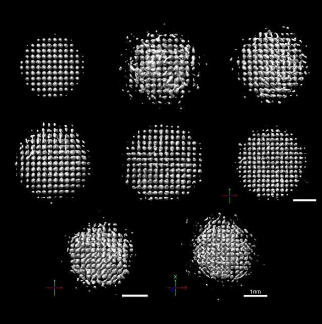
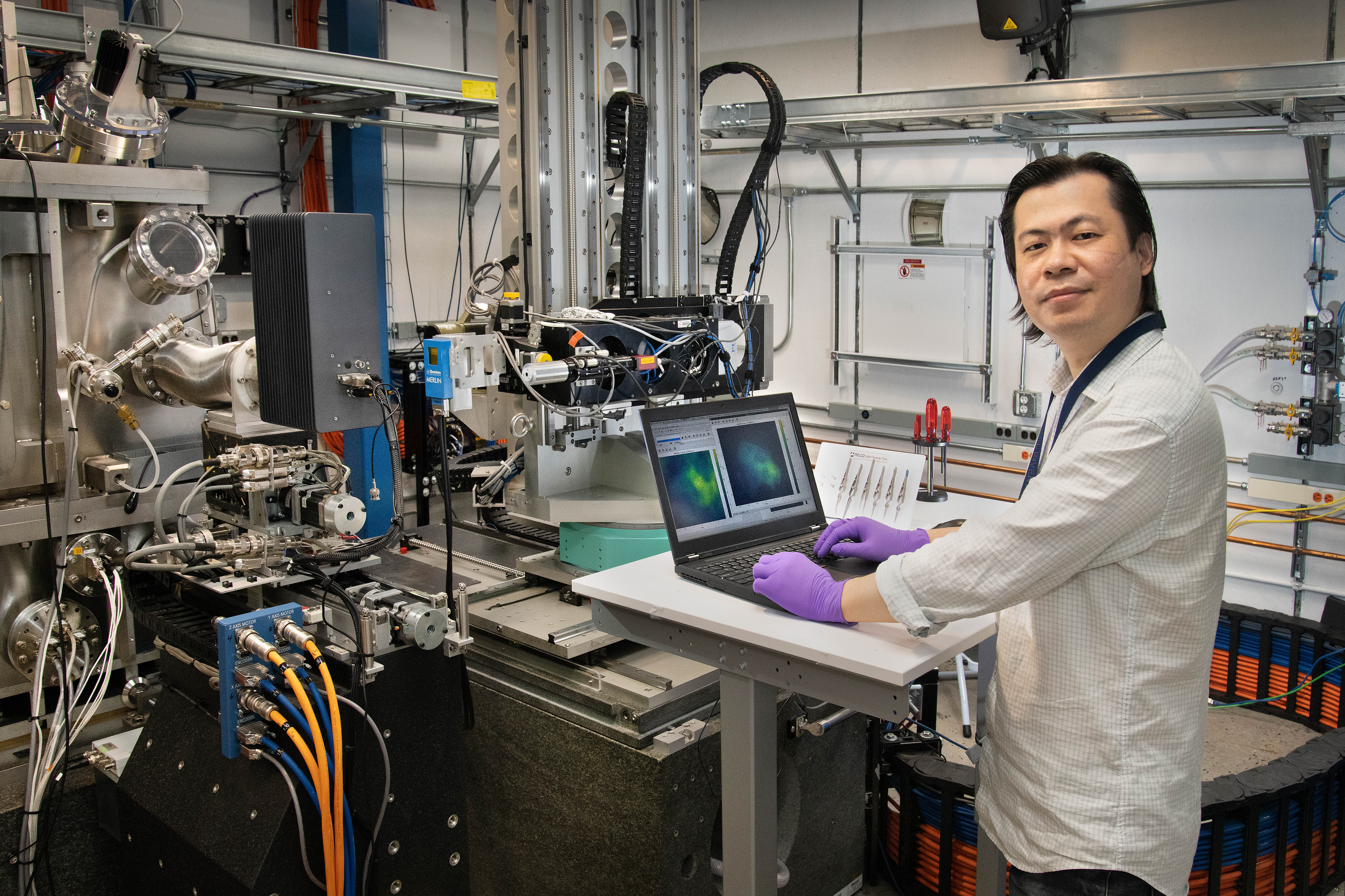
Science Snapshots from Berkeley Lab: 3D nanoparticles and magnetic spin
Researchers at Berkeley Lab have captured 3D images of nanoparticles in liquid with atomic precision, and developed an ultrathin electrical switch that could further miniaturize computing devices and personal electronics without loss of performance.
A Talented 2D Material Gets a New Gig
Berkeley Lab scientists tap into graphene’s hidden talent as an electrically tunable superconductor, insulator, and magnetic device for the advancement of quantum information science
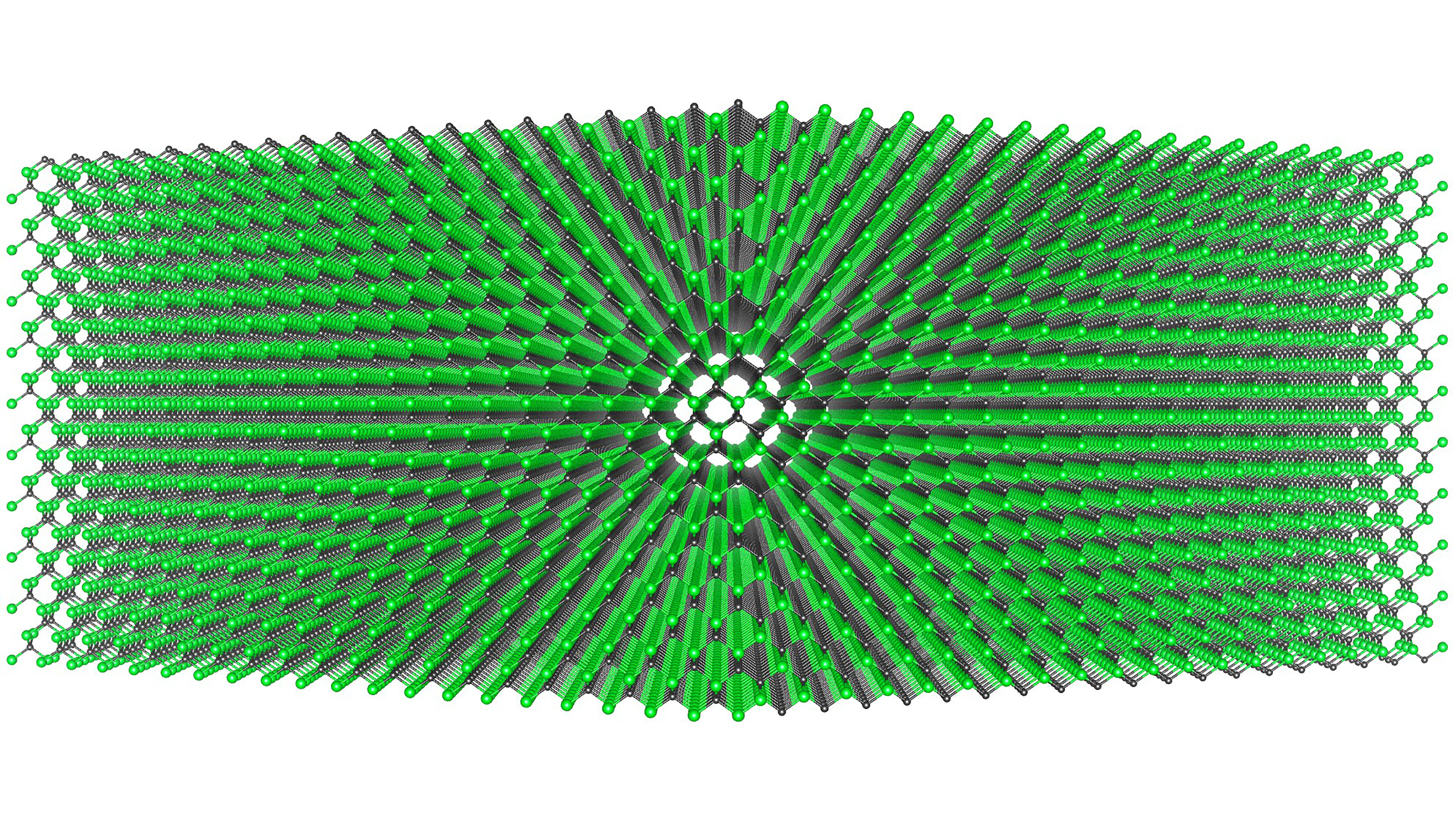
Living on the Edge: How a 2D Material Got Its Shape
A team of scientists led by the Department of Energy’s Lawrence Berkeley National Laboratory (Berkeley Lab) has gained valuable insight into 3D transition metal oxide nanoparticles’ natural “edge” for 2D growth.