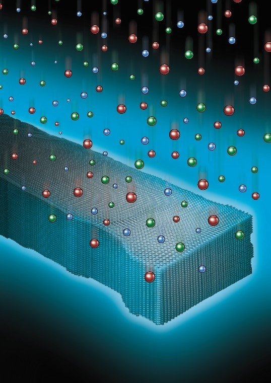
Scientists have developed a technique called plasmon engineering to create nanomaterials with near-atomic scale control of patterning in silicon. This new research used a specific plasmon engineering method, aberration-corrected electron beam lithography, to control the optical and electronic properties of silicon. This approach could one day be applied to industrial applications.