IBM is one company at the forefront of this movement, researching ways to shrink and redesign their microelectronics—the transistors and other semiconductor devices that make up the small but mighty chips at the heart of all consumer electronics.
“As devices get smaller, it becomes more challenging to maintain electrostatic control,” said Conal Murray, a scientist at IBM’s T.J. Watson Research Center. “To ensure we can deliver the same level of performance in smaller devices, we’ve been employing new semiconductor materials and designs over the last decade.”
One notable semiconductor design is IBM’s nanosheet-based architecture. Compared to typical, planar semiconductor designs, this 3-D architecture is an array of ultrathin, alternating material layers (nanosheets), sandwiched together and encapsulated to improve electrostatic control.
“By implementing this new architecture, we’ve also introduced materials to our devices that actually strain their surroundings,” Murray said.
While straining a material may sound like a negative effect, the mechanism is actually more complicated, offering significant benefits.
“Imagine you have a stack of tennis balls in a can,” Murray said. “If you squeeze the can, the position of each tennis ball will change slightly. This represents how the position of atoms within our semiconductor materials can be changed at a very local scale with strain. And because the position of atoms influences the device’s electronic properties, we can use strain to tailor those materials and get better device performance.”
Manipulating materials with strain is not a new concept; however, as electronic devices continually get smaller, it becomes more challenging to introduce the right amount of strain. “You have to make sure you can add enough stress without the tennis ball can opening up,” Murray said.
“At some point, if the strain is too big of a mismatch for the material, it will limit the lifetime of the transistor,” said Hanfei Yan, a scientist at the National Synchrotron Light Source II (NSLS-II), a U.S. Department of Energy (DOE) Office of Science User Facility at DOE’s Brookhaven National Laboratory.
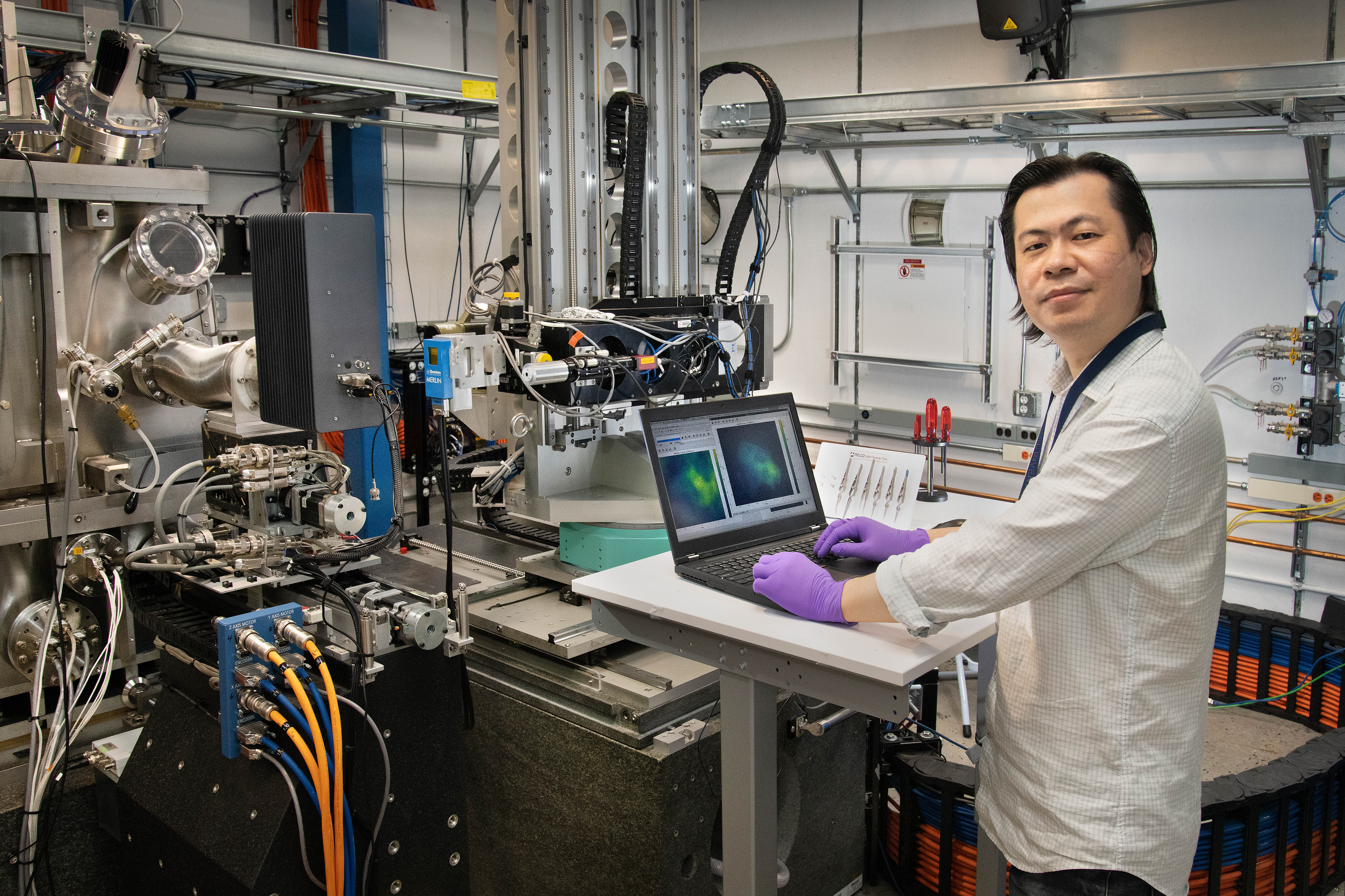
In order to tune materials through strain, researchers must first measure the strain on the nanoscale, and that’s a challenge in itself. Researchers must use a tool that is small enough to probe a structure that is just a few nanometers in size and sensitive enough to keep the original material properties intact. To study strain in their nanosheet architecture, IBM chose the Hard X-ray Nanoprobe (HXN) at NSLS-II.
“HXN offers a unique combination of capabilities that is not available anywhere else—the high penetration power of x-rays, NSLS-II’s ultrabright source, and the beamline’s small probe,” Yan said. “We have a special, in-house developed x-ray nanofocusing optic at HXN called the Multilayer Laue Lens that enables us to focus x-rays down to a very small spot—about 10 nanometers. Together, these capabilities enable us to precisely measure the strain in a tiny amount of material.”
By bringing their nanosheet architecture to NSLS-II, IBM was also able to study the device in its original state.
“The typical way that many researchers study their devices is to use a technique like electron microscopy, because that technique offers the best resolution,” Murray said. “The downside is that you have to remove a piece of your sample and thin it down so the electrons can pass through it. In each of those steps, you could be drastically altering the strain state of your original device. So another advantage of using synchrotron-based diffraction studies at NSLS-II is that we don’t have to tear apart our devices in order to examine them.”
Murray added, “HXN has been such a useful tool for us. We’re able to scan a single device or an array of devices, measure them under different conditions, and determine exactly what is happening in their native environments.”
As IBM measured the strain in their nanosheet architecture, NSLS-II revealed something surprising. Years prior, IBM had studied the strain in their materials at the microscale and observed a surface relaxation effect. They expected to see the same results at the nanoscale, but instead they saw the opposite effect.
“This is something that we probably could only see using HXN,” Murray said. “And it was exciting, particularly because the edges of the material contain the most current, and therefore most of the effects of the devices happen in those regions.”
The IBM researchers followed up the NSLS-II experiments with sophisticated mechanical modeling that confirmed the findings. The takeaways from NSLS-II will enable IBM to improve the performance of small electronic devices, pushing them to run faster while consuming less power.
This study was supported by IBM and the U.S. Department of Energy’s Office of Science.
Brookhaven National Laboratory is supported by the U.S. Department of Energy’s Office of Science. The Office of Science is the single largest supporter of basic research in the physical sciences in the United States and is working to address some of the most pressing challenges of our time. For more information, visit https://energy.gov/science.
Follow @BrookhavenLab on Twitter or find us on Facebook.