For scientists to probe materials with electron beams, they require software, such as the finite element for software called Computational Fluid Dynamics, used by Silviu Covrig Dusa to make precision measurements at the Thomas Jefferson National Accelerator Facility.
Tag: Electron Beam
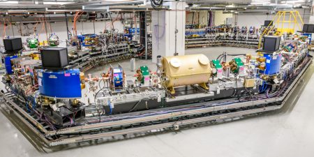
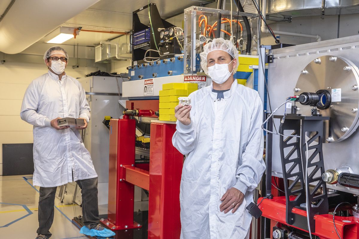
Experts Go All In when CEBAF Is in Trouble
What happens when a unique research machine breaks? The question isn’t academic. In April, sensors showed that a vacuum seal in Jefferson Lab’s Continuous Electron Beam Accelerator Facility had failed in a critical area of the injector – the chopper – where electrons are sorted by large copper cavities and directed for experiments. Without that vacuum seal, outside air we breathe will enter those cavities, contaminating the system and effectively crippling accelerator operations. An ad hoc team of experts from the accelerator and engineering divisions assembled to diagnose the situation and figure out how to fix it.
New Dual-Beam Microscope Installed at the Center for Functional Nanomaterials
This latest-generation tool, which combines a scanning electron microscope and focused-ion beam, has advanced capabilities for preparing and analyzing nanomaterial samples.
Method for determining electron beam properties could help future ultraviolet, X-ray synchrotron light sources
Fermilab user and University of Chicago PhD candidate Ihar Lobach explains how his team used Fermilab’s IOTA electron storage ring to glean insights that can be difficult to obtain on an electron beam and how this proof of principle could benefit the Advanced Photon Source Upgrade at Argonne National Laboratory.
A New Way to Measure Record-Setting Electron Beams
A new, compact system has been successfully demonstrated at the Berkeley Lab Laser Accelerator (BELLA) Center to provide simultaneous high-resolution measurements of multiple electron-beam properties.
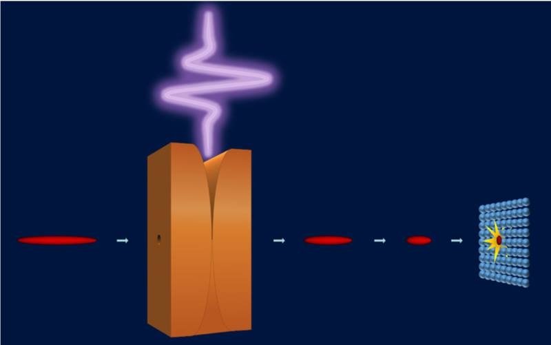
Laser-Driven “Chirp” Powers High-Resolution Materials Imaging
Scientists use beams of electrons to study materials’ properties. Shorter beams produce higher-resolution views. To make shorter beams, the electrons at the tail of the beam need to catch up to the head of the beam. This is accomplished by giving the electrons at the tail extra energy, a so-called “energy chirp.” Scientists have now used a terahertz laser pulse to create this energy chirp.
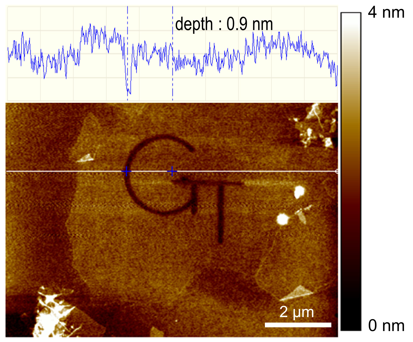
E-Beam Atomic-scale 3-D “Sculpting” Could Enable New Quantum Nanodevices
By varying the energy and dose of tightly-focused electron beams, researchers have demonstrated the ability to both etch away and deposit high-resolution nanoscale patterns on two-dimensional layers of graphene oxide. The 3D additive/subtractive “sculpting” can be done without changing the chemistry of the electron beam deposition chamber, providing the foundation for building a new generation of nanoscale structures.
‘Blinking” Crystals May Convert CO2 into Fuels
Imagine tiny crystals that “blink” like fireflies and can convert carbon dioxide, a key cause of climate change, into fuels. A Rutgers-led team has created ultra-small titanium dioxide crystals that exhibit unusual “blinking” behavior and may help to produce methane and other fuels, according to a study in the journal Angewandte Chemie. The crystals, also known as nanoparticles, stay charged for a long time and could benefit efforts to develop quantum computers.
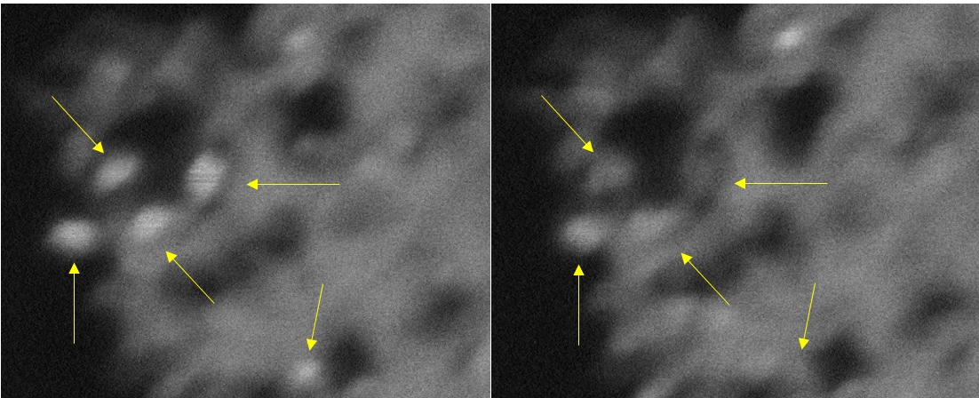
A Study Provides New Insights Into van der Waals Materials
Van der Waals materials that are layered on top of each other are of high interest for electronic and photonic applications. A recent study by Penn State and SLAC National Accelerator Laboratory, in California, provides new insights into the interactions of layered materials with laser and electron beams.

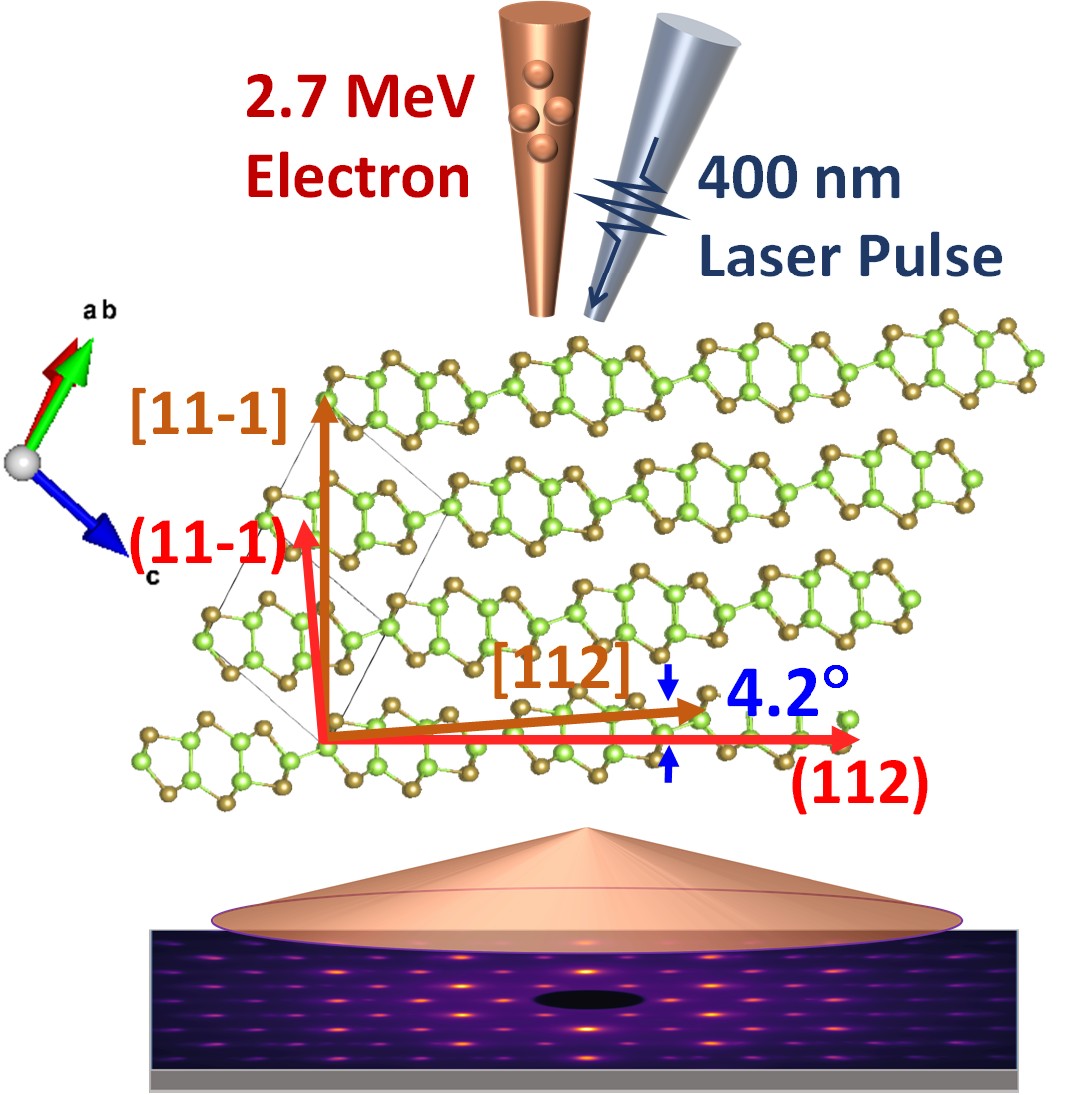
Pulsed Electron Beams Provide a Softer Touch for Atomic-Scale Imaging
A team developed a method to apply pulsed-electron beams to image the beam-sensitive material with atomic resolution.