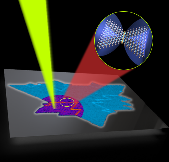
Two-dimensional quantum materials provide a unique platform for new quantum technologies, because they offer the flexibility of combining different monolayers featuring radically distinct quantum states. Different two-dimensional materials can provide building blocks with features like superconductivity, magnetism, and topological matter.…
Tag: 2D materials
Breaking boundaries in quantum photonics: Groundbreaking nanocavities unlock new frontiers in light confinement
In a significant leap forward for quantum nanophotonics, a team of European and Israeli physicists, introduces a new type of polaritonic cavities and redefines the limits of light confinement. This pioneering work, detailed in a study published today in Nature Materials, demonstrates an unconventional method to confine photons, overcoming the traditional limitations in nanophotonics.
Making Big Leaps in Understanding Nanoscale Gaps
Creating novel materials by combining layers with unique, beneficial properties seems like a fairly intuitive process—stack up the materials and stack up the benefits.
New Ultrathin Capacitor Could Enable Energy-Efficient Microchips
Scientists at Berkeley Lab and UC Berkeley have developed a thin film from a century-old material for next-gen memory and logic devices. The breakthrough advances the pursuit of low-voltage electronics that require less energy to operate than today’s silicon-based electronics.
CityU co-hosts online science and tech conference with Nature journals; pre launch for CityU’s HK Tech Forum
Leading scientists exchanged innovative views on contemporary trends in the chemistry of 2D materials at a three-day online conference co-organised by City University of Hong Kong (CityU) and Nature Conferences, the preeminent series curated by the highly prestigious science journal Nature and Nature journals.
Skyrmions on the Rise – New 2D Material Advances Low-Power Computing
A team co-led by Lawrence Berkeley National Laboratory has discovered a new ultrathin material with exotic magnetic features called skyrmions. The new material could enable the next generation of tiny, fast, energy-efficient electronic devices.
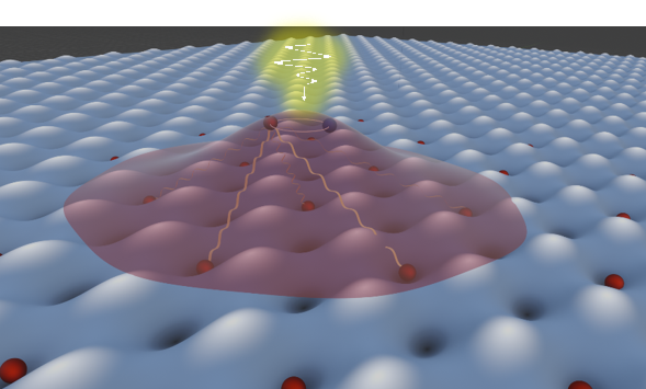
Lasers trigger magnetism in atomically thin quantum materials
Researchers discovered that light can trigger a form of magnetism in a normally nonmagnetic material. This magnetism centers on the behavior of electron “spin.” By controlling & aligning electron spin at this level of detail & accuracy, this platform could have applications in quantum computing & simulation.
Zhongwei Dai: Exploring the Strange Quantum World of 2D Materials
Zhongwei Dai, a researcher in the Interface Science and Catalysis Group of the Center for Functional Nanomaterials, probes the properties of atomically thin materials to identify promising candidates for quantum information science applications
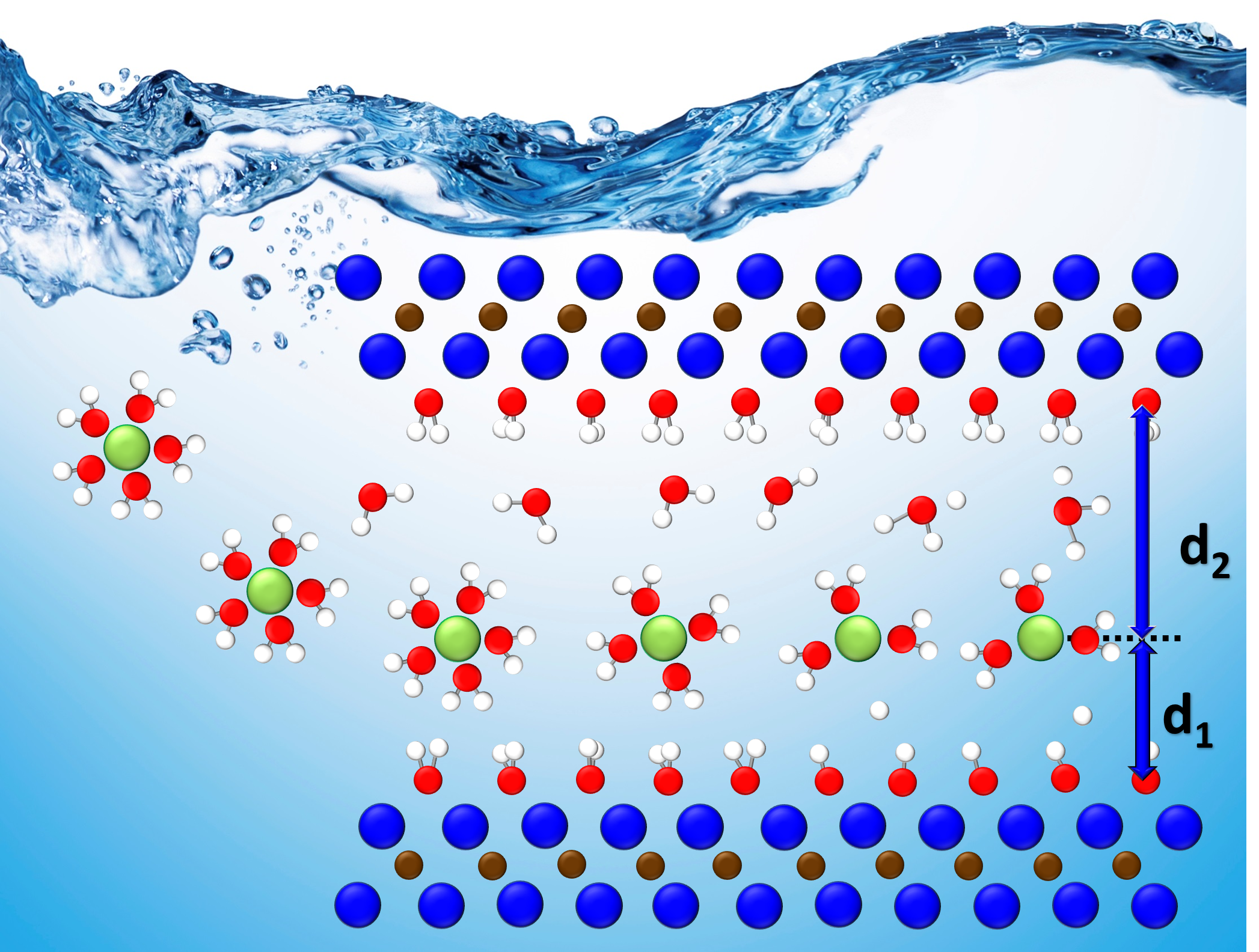
A simple way to get complex semiconductors to assemble themselves
A new way to make complex, layered semiconductors is like making rock candy: They assemble themselves from chemicals in water. The method will aid design and large-scale production of these materials.
One scientist’s trash is another’s treasure:
While making materials samples to pursue their own research goals, scientists at the U.S. Department of Energy’s Ames Laboratory discovered that an unwanted byproduct of their experiments was an extremely high-quality and difficult-to-obtain substance sought after by scientists researching layered materials.
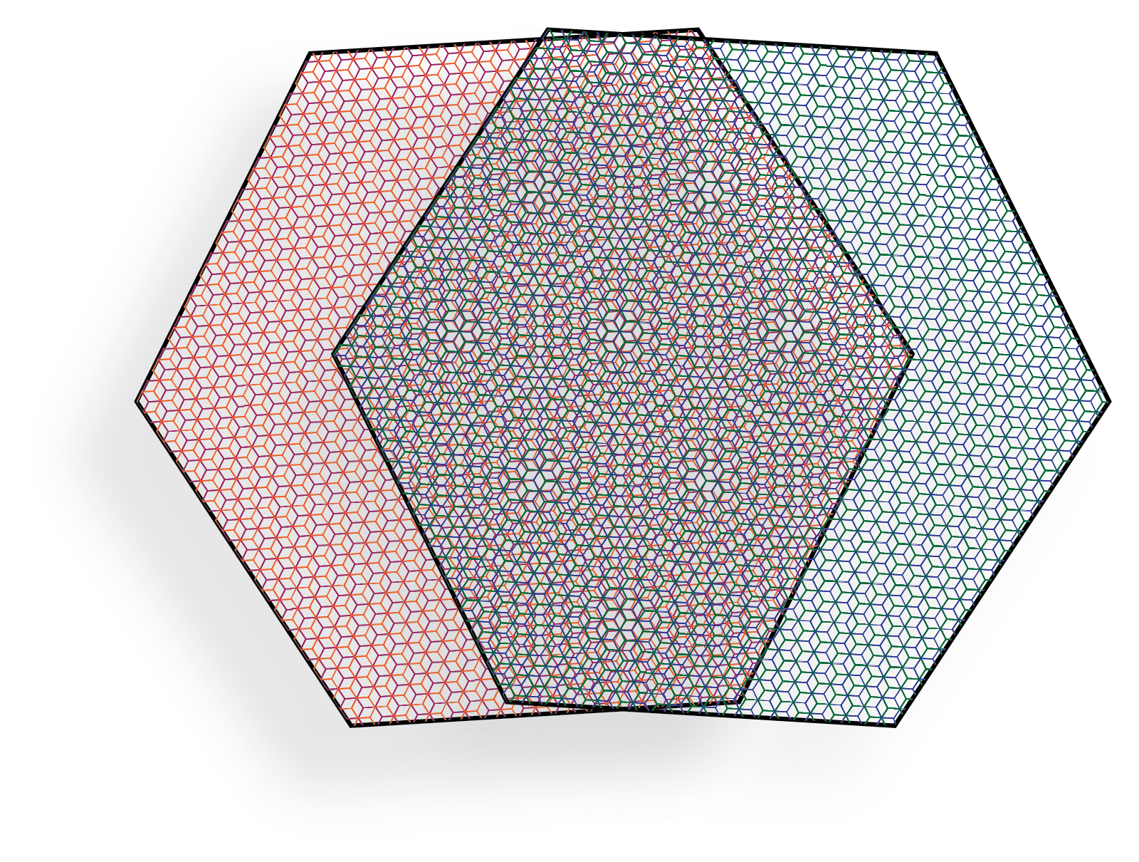
Layered Graphene with a Twist Displays Unique Quantum Confinement in 2-D
Bilayer graphene with one of the two layers twisted displayed unique resonant electronic behavior. Understanding how electrons move in such 2-D materials could shed light on how to manipulate them for quantum computing and communication.
National 2D materials research center wins NSF funding
Operated by Penn State University’s Materials Research Institute in partnership with Rice University, ATOMIC has won $1.5 million in Phase II funding that will allow it to add both a new academic partner, Boise State University, and new industry partners. ATOMIC currently has 13 industry partners and five government partners.
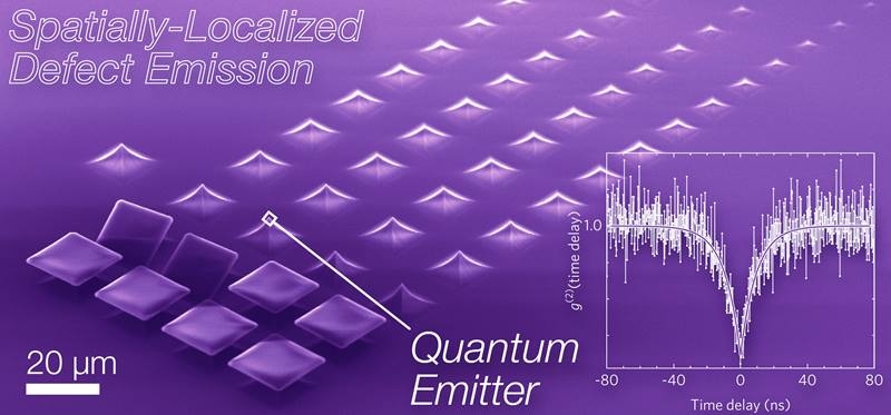
Finding new types of 2D material defects could enable better electronics
The discovery of new types of defects in 2D materials may lead to the creation of new ultra-compact electronic devices.
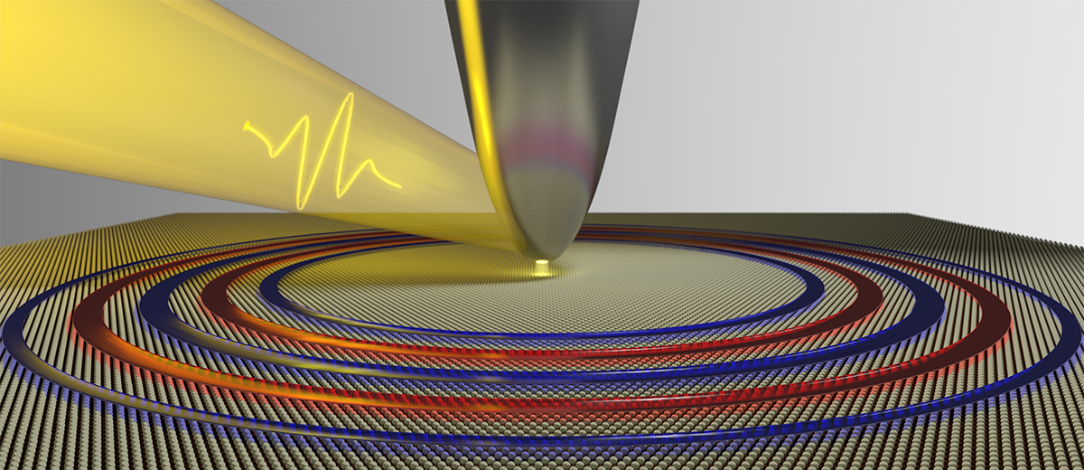
A Spatiotemporal Symphony of Light
Using an ultrafast transmission electron microscope, researchers from the Technion – Israel Institute of Technology have, for the first time, recorded the propagation of combined sound and light waves in atomically thin materials.
NSF renews funding for Two-Dimensional Crystal Consortium
The National Science Foundation (NSF) announced a renewal of funding for the Materials Innovation Platform (MIP) national user facility at Penn State’s Materials Research Institute (MRI), the Two-Dimensional Crystal Consortium (2DCC). The 2DCC is one of four MIPs in the United States and was awarded $20.1 million over five years, an increase of 13% above the initial award in 2016.
NUS scientists create a new type of intelligent material
Researchers from the National University of Singapore have created a new class of intelligent materials. It has the structure of a two-dimensional (2D) material, but behaves like an electrolyte – and could be a new way to deliver drugs within the body.
April Snapshots
Science Snapshots from Berkeley Lab: X-rays accelerate battery R&D; infrared microscopy goes off grid; substrates support 2D tech

Science Snapshots From Berkeley Lab – Week of March 29, 2021
India’s Ambitious Clean Energy Goals, a Secret Pathway to Harnessing the Sun for Clean Energy, and a Supersmart Gas Sensor for Asthmatics
All together now: Experiments with twisted 2D materials catch electrons behaving collectively
A team led by the University of Washington reports that carefully constructed stacks of graphene — a 2D form of carbon — can exhibit highly correlated electron properties. The team also found evidence that this type of collective behavior likely relates to the emergence of exotic magnetic states.
Science Snapshots September 2020
2D Electronics, Plant Biofactories, Transforming Waste, and Vaccine Development.
Faster, more efficient energy storage could stem from holistic study of layered materials
A team led by Oak Ridge National Laboratory developed a novel, integrated approach to track energy-transporting ions within an ultra-thin material, which could unlock its energy storage potential leading toward faster charging, longer lasting devices.
2D Electronics Get an Atomic Tuneup
Scientists at Berkeley Lab have demonstrated a new technique that could improve the performance of atomically thin semiconductors for next-generation electronics such as optoelectronics, thermoelectrics, and sensors.

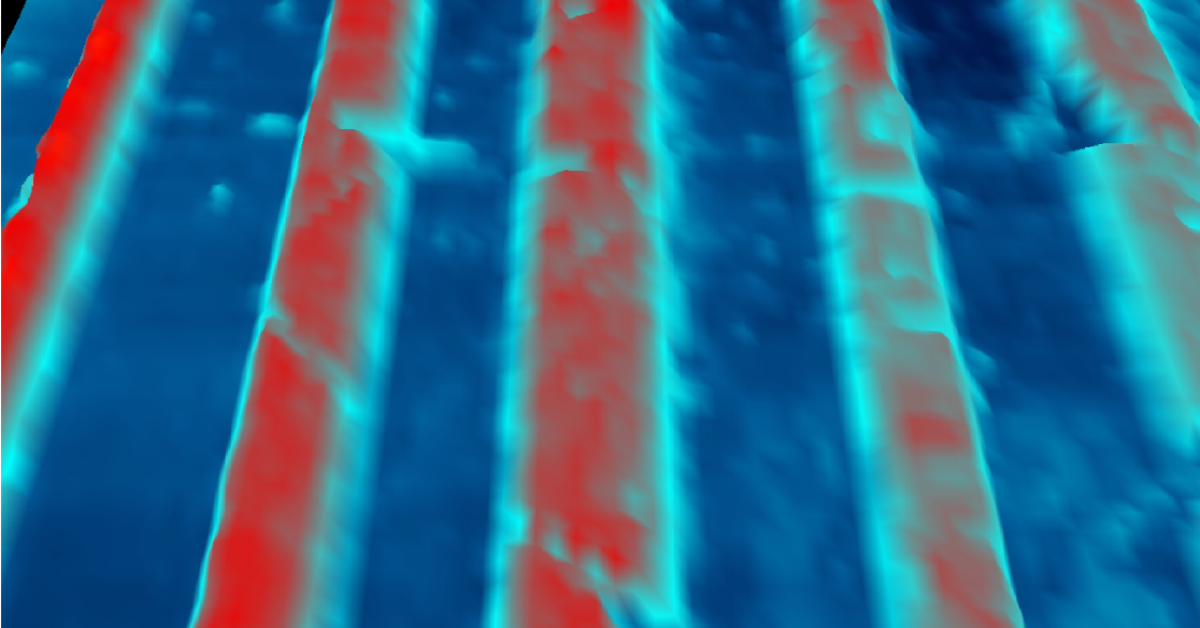
Quantum Materials Quest Could Benefit From Graphene That Buckles
Graphene, an extremely thin two-dimensional layer of the graphite used in pencils, buckles when cooled while attached to a flat surface, resulting in beautiful pucker patterns that could benefit the search for novel quantum materials and superconductors, according to Rutgers-led research in the journal Nature. Quantum materials host strongly interacting electrons with special properties, such as entangled trajectories, that could provide building blocks for super-fast quantum computers. They also can become superconductors that could slash energy consumption by making power transmission and electronic devices more efficient.
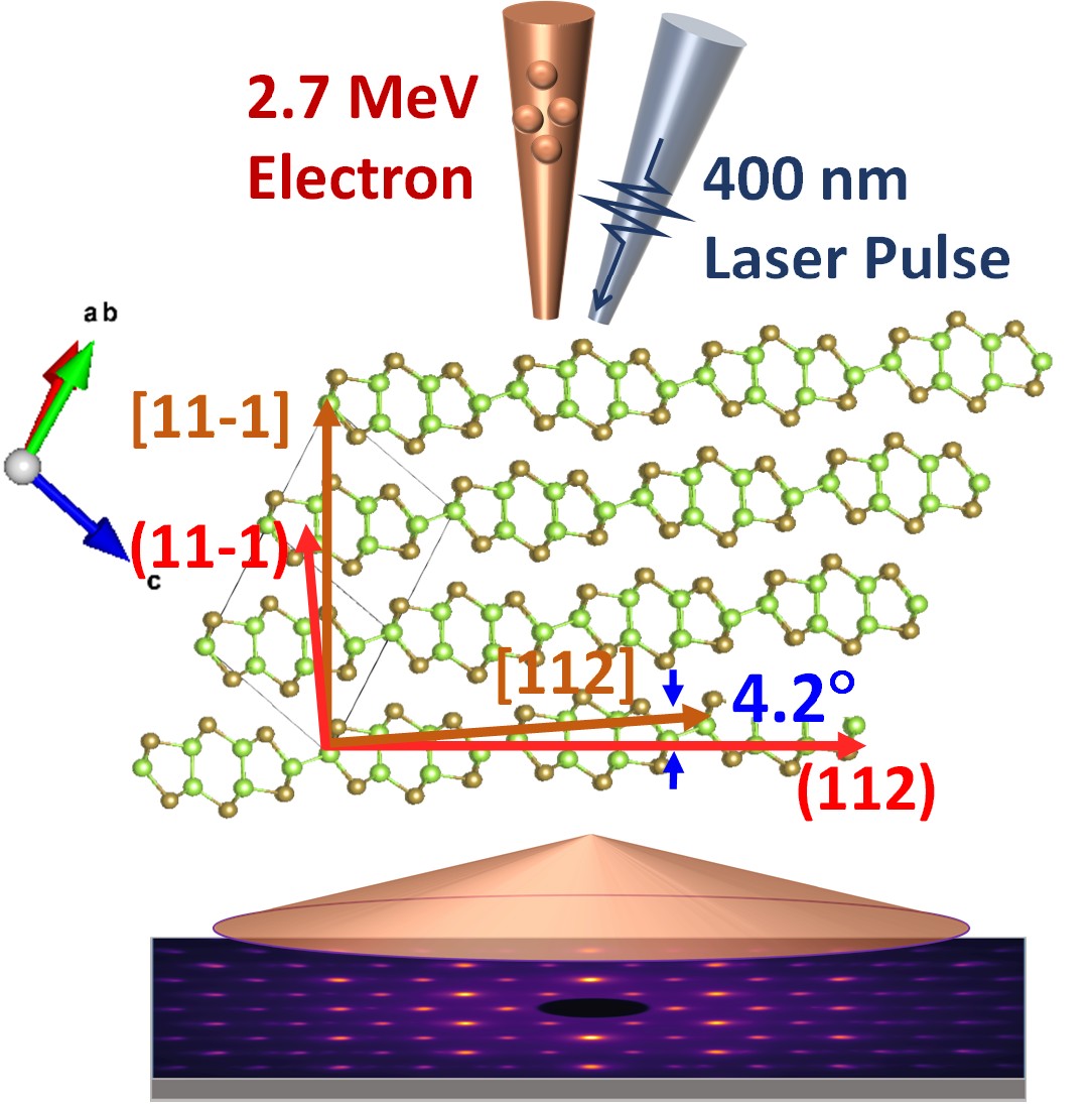
A Study Provides New Insights Into van der Waals Materials
Van der Waals materials that are layered on top of each other are of high interest for electronic and photonic applications. A recent study by Penn State and SLAC National Accelerator Laboratory, in California, provides new insights into the interactions of layered materials with laser and electron beams.
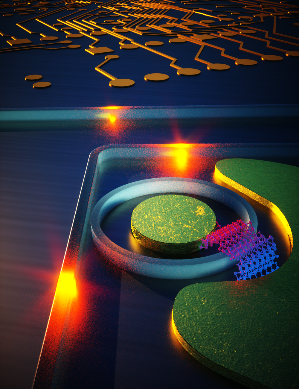
Strainoptronics: A New Way to Control Photons
SUMMARYResearchers discovered a new way to engineer optoelectronic devices by stretching a two-dimensional material on top of a silicon photonic platform. Using this method, coined strainoptronics by a team led by George Washington University professor Volker Sorger, the researchers demonstrated…
NUS researchers develop a new library of atomically thin 2D materials
Researchers from the National University of Singapore have created a new collection of atomically thin two-dimensional materials. Using novel synthesis conditions for transition metal dichalcogenides, more than 10 new materials have been made by the team, with many more still to be discovered.
Making Quantum ‘Waves’ in Ultrathin Materials
A team of researchers co-led by Berkeley Lab has observed unusually long-lived wavelike electrons called “plasmons” in a new class of electronically conducting material. Plasmons are very important for determining the optical and electronic properties of metals.
Preventing metal pipe corrosion
A thin, single layer of graphene material only 1 atom thick may reduce metal pipe corrosion rates as much as 100 times. These new crystalline 2D materials could mean big savings to industries.

Smithsonian Releases 2.8 Million Free Images for Broader Public Use
The Smithsonian announced today the launch of Smithsonian Open Access, an initiative that removes Smithsonian copyright restrictions from about 2.8 million of its digital collection images and nearly two centuries of data. This means that people everywhere can now download, transform and share this open access content for any purpose, for free, without further permission from the Smithsonian.
When Bonding Noble Metals to 2D Materials, Interfaces Matter
Researchers at Penn State and Purdue University have developed new materials for improved single-atom catalysis and future electronics.
No Strain, No Gain! Breakthrough in 2D Material that Produces Single Photons
Recent research has shown that 2D materials may have potential as light sources that emit light as single photons.
New Method to Detect Defects in 2D Materials for Future Electronics, Sensors
A team of researchers from Penn State, Northeastern University, Rice University and Universidade Federal de Minas Gerais in Brazil have developed a technique to quickly and sensitively characterize defects in 2D materials.

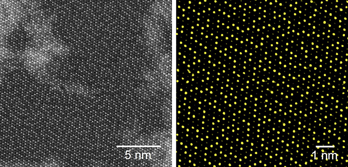
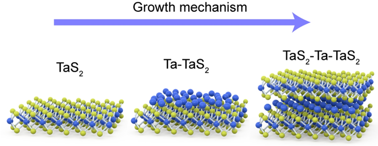
The Beauty of Imperfections: Linking Atomic Defects to 2D Materials’ Electronic Properties
Scientists at Berkeley Lab have revealed how atomic defects emerge in transition metal dichalcogenides, and how those defects shape the 2D material’s electronic properties. Their findings could provide a versatile yet targeted platform for designing 2D materials for quantum information science.
How do you know it’s perfect graphene?
Scientists at the U.S. Department of Energy’s Ames Laboratory have discovered an indicator that reliably demonstrates a sample’s high quality, and it was one that was hiding in plain sight for decades.