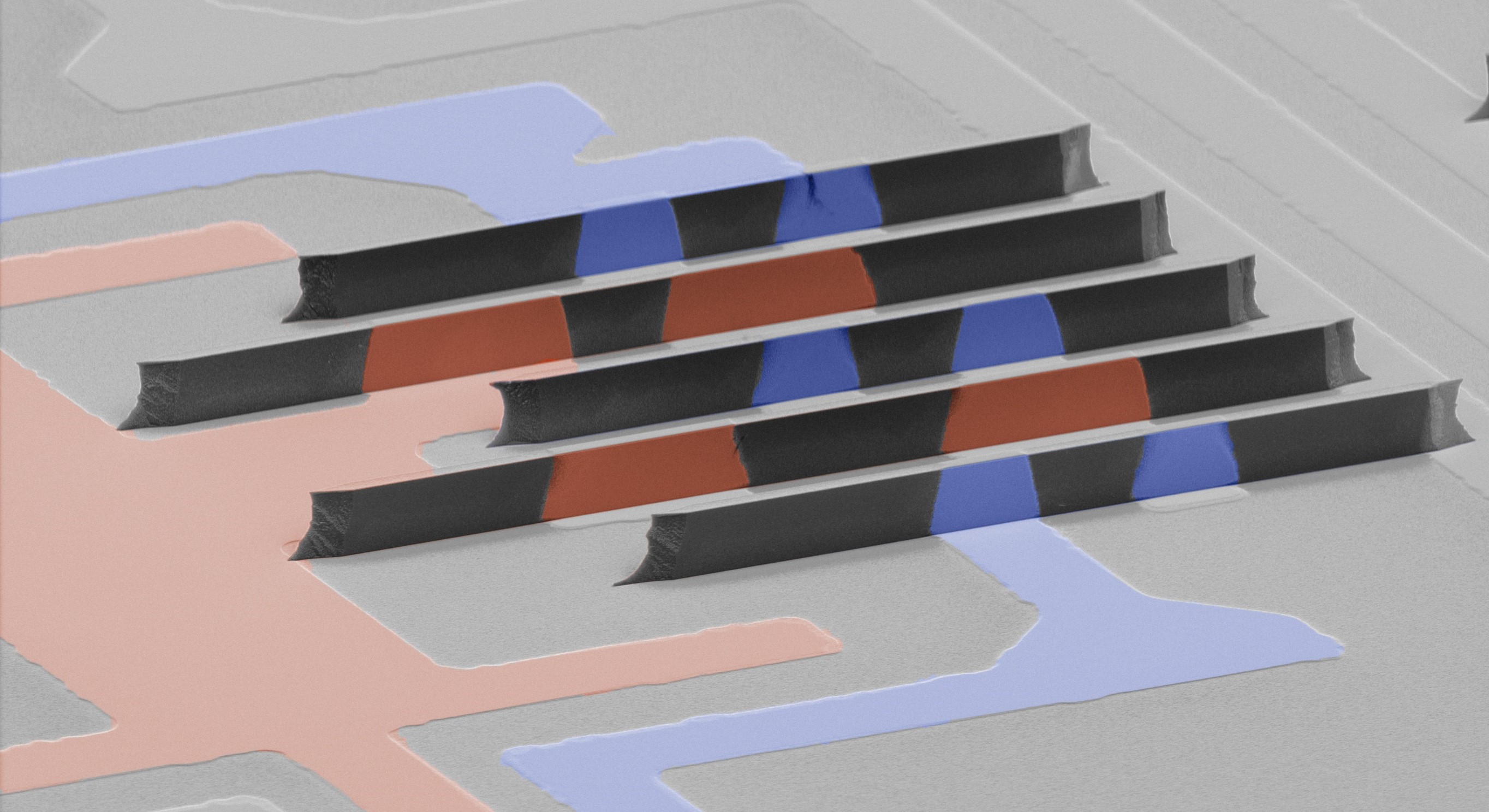
Scientists at the University of Florida have pioneered a method for using semiconductor technology to manufacture processors that significantly enhance the efficiency of transmitting vast amounts of data across the globe.
news, journals and articles from all over the world.
Scientists at the University of Florida have pioneered a method for using semiconductor technology to manufacture processors that significantly enhance the efficiency of transmitting vast amounts of data across the globe.
Scientists have demonstrated “multielement ink” – the first “high-entropy” semiconductor that can be processed at low-temperature or room temperature. The new material could enable cost-effective and energy-efficient semiconductor manufacturing.
The new school will integrate academic programs and manufacturing research to meet the challenges of Industry 4.0.
Scientists at Berkeley Lab and UC Berkeley have developed a thin film from a century-old material for next-gen memory and logic devices. The breakthrough advances the pursuit of low-voltage electronics that require less energy to operate than today’s silicon-based electronics.
Some analysts say that the end of Moore’s Law is near, but Patrick Naulleau, the director of Berkeley Lab’s Center for X-Ray Optics (CXRO), says that it could be decades before the modern chip runs out of room for improvement, thanks to advances in materials and instrumentation enabled by the CXRO.
A process for making hybrid organic-inorganic materials (photoresists) sensitive to extreme-ultraviolet (EUV) light is one of two technologies that won the 2021 National Labs Accelerator Pitch Event. This technology—developed at the Center for Functional Nanomaterials (CFN), a U.S. Department of Energy (DOE) Office of Science User Facility at Brookhaven National Laboratory—could be used for next-generation semiconductor manufacturing by EUV lithography.
The Princeton Plasma Physics Laboratory has appointed David Graves, an internationally known chemical engineer, to head a new research enterprise that will explore plasma applications in semiconductor manufacturing and the next generation of super-fast quantum computers.