Scientists at Berkeley Lab and UC Berkeley have developed a nanoparticle composite that grows into 3D crystals. The new 3D-grown material could speed up production and eliminate errors in the mass manufacturing of nanoscale photonics for smart buildings or actuators for robotics.
Tag: Crystal
A new ‘gold standard’ compound for generating electricity from heat
Researchers show in a new study that a single material, a layered crystal consisting of the elements rhenium and silicon, turns out to be the gold standard of transverse thermoelectric devices.
Revealing Nano Big Bang – Scientists Observe the First Milliseconds of Crystal Formation
At Berkeley Lab’s Molecular Foundry, scientists recruited a world-leading microscope to capture atomic-resolution, high-speed images of gold atoms self-organizing, falling apart, and then reorganizing many times before settling into a stable, ordered crystal.

Emerging Wide Bandgap Semiconductor Devices Based on Silicon Carbide May Revolutionize Power Electronics
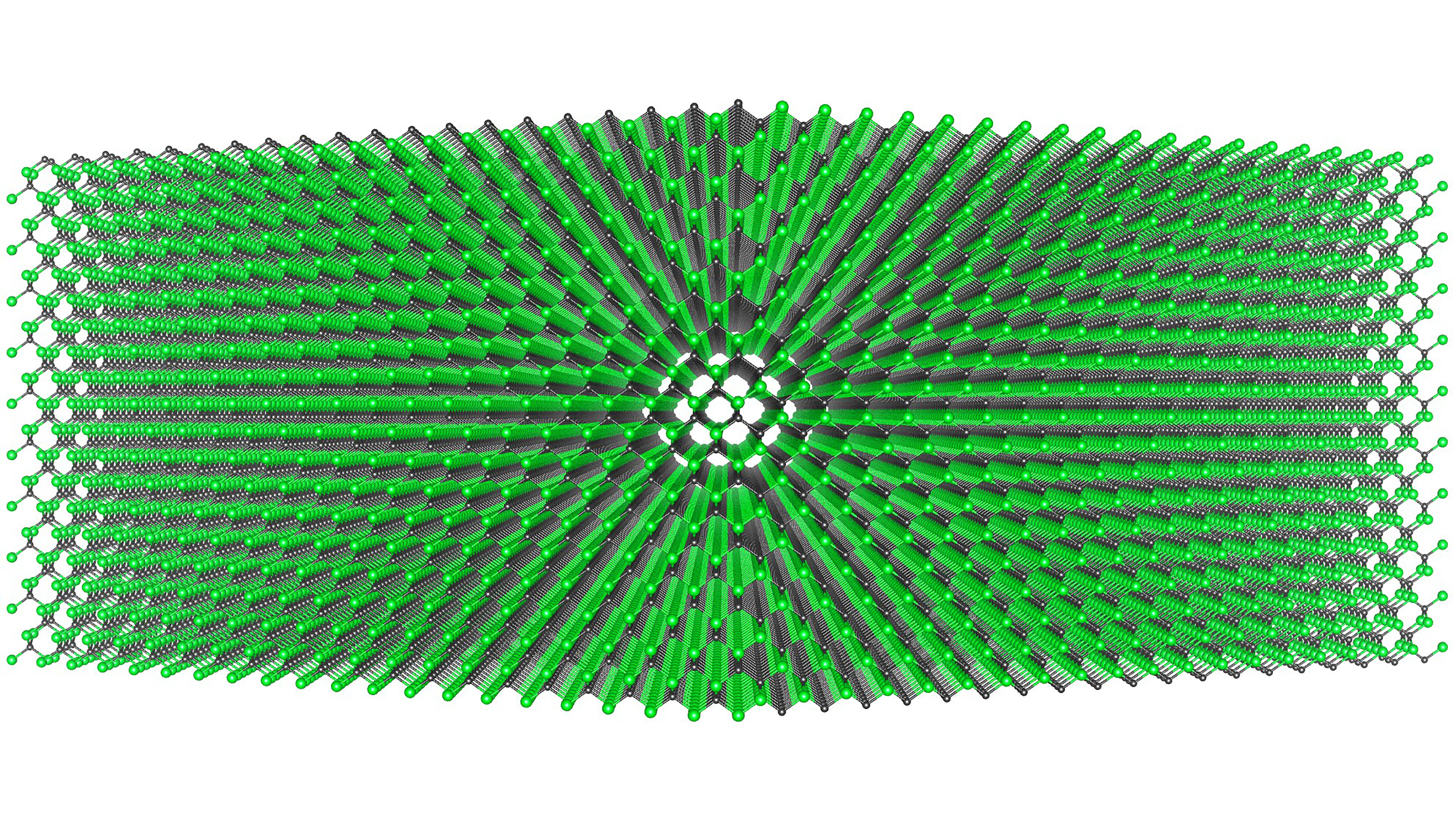
Silicon plays a central role within the semiconductor industry for microelectronic and nanoelectronic devices, and silicon wafers of high purity single-crystalline material can be obtained via a combination of liquid growth methods. In Applied Physics Reviews, researchers describe the atomic mechanisms governing extended defect kinetics in cubic silicon carbide, which has a diamondlike zincblende crystal structure that manifests stacking and anti-phase instabilities. The study pinpoints the atomistic mechanisms responsible for extended defect generation and evolution.