In a paper published today in Nature Photonics, researchers from the University of Oxford, along with collaborators from the Universities of Muenster, Heidelberg, and Exeter, report on their development of integrated photonic-electronic hardware capable of processing three-dimensional (3D) data, substantially boosting data processing parallelism for AI tasks.
Tag: Photonics
New loss mitigation technique paves the way for perfect optical resonators
Optical resonators are used in everything from familiar laser pointers to cutting-edge photonic quantum computers. But they all suffer from losses that degrade their performance. Researchers at Aalto University have now developed a way to prevent those losses, boosting the…
Discovery may lead to terahertz technology for quantum sensing
Visible light is a mere fraction of the electromagnetic spectrum, and the manipulation of light waves at frequencies beyond human vision has enabled such technologies as cell phones and CT scans. Rice University researchers have a plan for leveraging a previously unused portion of the spectrum.
Transferring Data with Many Colors of Light Simultaneously
The Lightwave Research Lab has developed a fast and extremely efficient method for transferring huge amounts of data. The technique uses dozens of frequencies of light to transfer several streams of information over a fiber optic cable simultaneously.
Researchers demonstrate noise-free communication with structured light
Researchers at the University of the Witwatersrand (Wits) have outlined a new optical communication protocol that exploits spatial patterns of light for multi-dimensional encoding in a manner that does not require the patterns to be recognised, thus overcoming the prior limitation of modal distortion in noisy channels.
Rutgers is Part of NSF-funded Consortium to Advance Photonics Research and Workforce Development
Rutgers is part of a new federally funded regional collaboration to drive economic and technological advancements in photonics, the National Science Foundation (NSF) announced. The consortium, which includes researchers from Rutgers-Newark and Rutgers-New Brunswick, awarded a development grant from the NSF’s Regional Innovation Economic Engine consortium, led by Princeton University and co-led by Rowan University, with partners throughout New Jersey and neighboring states Delaware, Pennsylvania and New York.
Counting Photons for Quantum Computing
Experts in nuclear physics and quantum information have demonstrated the application of a photon-number-resolving system to accurately resolve more than 100 photons. The feat is a major step forward in capability for quantum computing development efforts. It also may enable quantum generation of truly random numbers, a long-sought goal for developing unbreakable encryption techniques for applications in, for instance, military communications and financial transactions.
Argonne aids in the fight against one of the world’s most ubiquitous human viruses
With the help of Argonne National Laboratory, Epstein-Barr Virus researchers identified a viral protein as a target for antiviral and vaccine development, as well as an antibody that might benefit the immunocompromised.
A new type of photonic time crystal gives light a boost
Smart surfaces mimic elusive photonic time crystals
Using X-rays and additive manufacturing to print tough materials
In a breakthrough for industrial manufacturing, scientists using the resources at Argonne were able to consistently produce 17-4 PH steel, one of the world’s toughest materials, using X-rays and the additive manufacturing process.
Hotter than infinity – light pulses can behave like an exotic gas
In the issue of the renowned journal Science published today (10.3.23), the team led by Prof. Dr Ulf Peschel reports on measurements on a sequence of pulses that travel thousands of kilometres through glass fibres that are only a few microns thin.
Teaching photonic chips to learn
A multi-institution research team has developed an optical chip that can train machine learning hardware.
Silicon photonic MEMS take a step forward
In recent years, global digitalization has seen unprecedented acceleration. Video streaming and video conferencing in home office and remote learning settings has resulted in a spike in residential broadband usage.
Tapping hidden visual information: An all-in-one detector for thousands of colours
A new chip from Aalto University researchers puts photonic information at our fingertips.

Yang wins Friedrich Wilhelm Bessel Research Award
The McKelvey School of Engineering’s Lan Yang has been selected to receive the Friedrich Wilhelm Bessel Research Award. Given by the Alexander von Humboldt Foundation, the award recognizes distinguished scientists in any discipline.
Latest Development of Meta-Devices: From Sensing and Imaging to Quantum Optical Chip
Professor Din-Ping Tsai, the Chair Professor of the Department of Electrical Engineering at the City University of Hong Kong (CityU), gave an online talk as part of the Hong Kong Institute for Advanced Study (HKIAS) Distinguished Lecture Series on Electronics and Photonics on 30 March 2022, titled “Meta-Devices: From Sensing and Imaging to Quantum Optical Chip”. Professor Hon Yan, Wong Chun Hong Professor of Data Engineering was the moderator.
One-dimensional red phosphorous glows in unexpected ways
In a study published in Nature Communications, an international team led by Aalto University researchers has found that fibrous red phosphorous, when electrons are confined in its one-dimensional sub-units, can show large optical responses – that is, the material shows strong photoluminescence under light irradiation. Red phosphorous, like graphene, belongs to a unique group of materials discovered in 2017 called one-dimensional van der Waals (1D vdW) materials.
Metamaterials research challenges fundamental limits in photonics
Cornell researchers are proposing a new way to modulate both the absorptive and the refractive qualities of metamaterials in real time, and their findings open intriguing new opportunities to control, in time and space, the propagation and scattering of waves for applications in various areas of wave physics and engineering.
This crystal impurity is sheer perfection
Scientists at Berkeley Lab and UC Berkeley have developed a nanoparticle composite that grows into 3D crystals. The new 3D-grown material could speed up production and eliminate errors in the mass manufacturing of nanoscale photonics for smart buildings or actuators for robotics.
Flexible, easy-to-scale nanoribbons move graphene toward use in tech applications
In a study published April 16 in ACS Photonics, University of Wisconsin–Madison researchers fabricated graphene into the smallest ribbon structures to date using a method that makes scaling-up simple. In tests with these tiny ribbons, the scientists discovered they were closing in on the properties they needed to move graphene toward usefulness in telecommunications equipment.
Brookhaven Lab and Northrop Grumman to Further Lab-Industry Collaborations
Through the U.S. Department of Energy’s Technologist in Residence program, Brookhaven Lab and Northrop Grumman scientists will partner on quantum materials research.
Caught in the act: New data about COVID-19 virus’s functions could aid in treatment designs
For the first time, a team of researchers has captured X-ray images of a critical enzyme of the COVID-19 virus performing its function. This discovery could improve design of new treatments against the disease.
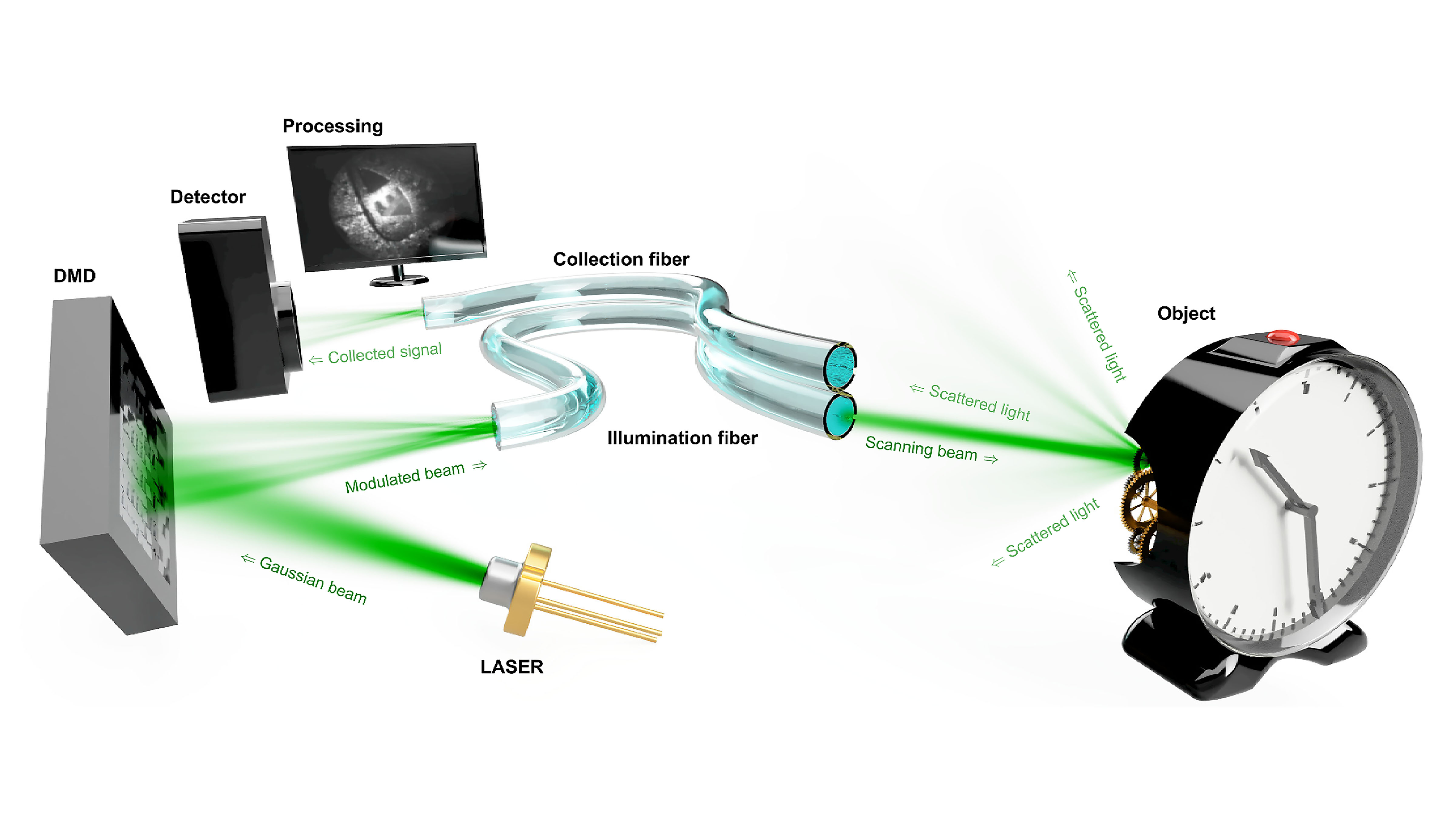
Using Holographic Endoscopes to Observe Distant Objects
Scientists are developing tools to observe the biological machinery in in vivo animal models to be able to understand and better treat severe brain diseases, and holographic endoscopes attracted interest because of their potential to conduct minimally invasive observations. In APL Photonics, researchers in Germany created a particularly narrow endoscope made of single hair-thin optical fibers that uses holographic methods to reconstruct images of macroscopic objects placed in front of the far end of the endoscope.
Twistoptics—A New Way to Control Optical Nonlinearity
Columbia Engineering researchers report that they developed a new, efficient way to modulate and enhance an important type of nonlinear optical process: optical second harmonic generation—where two input photons are combined in the material to produce one photon with twice the energy—from hexagonal boron nitride through micromechanical rotation and multilayer stacking. Their work is the first to exploit the dynamically tunable symmetry of 2D materials for nonlinear optical applications.
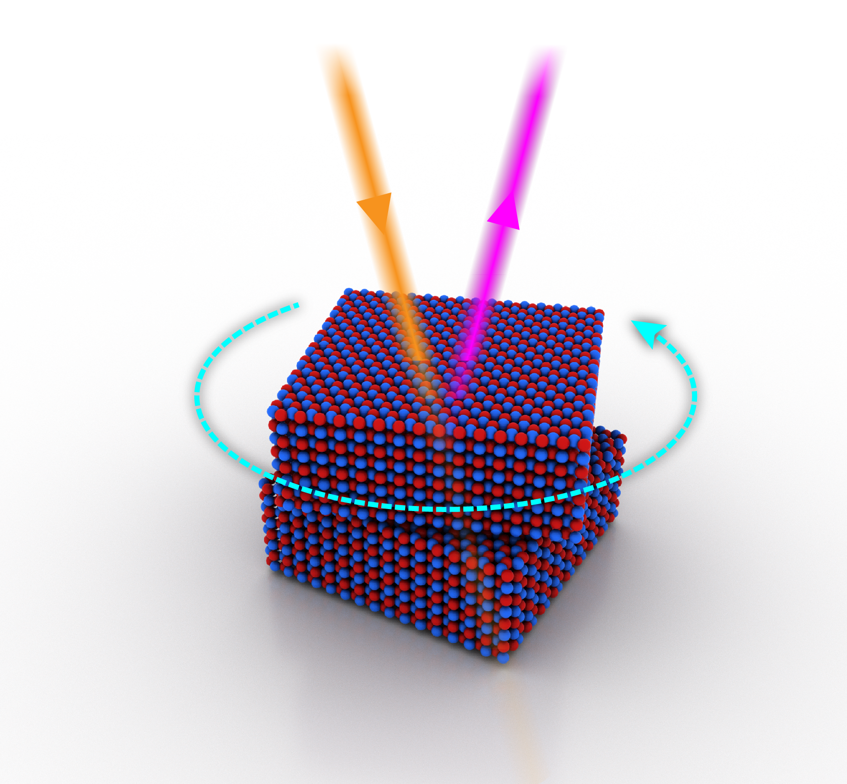
Molybdenum Disulfide Ushers in Era of Post-Silicon Photonics
Researchers of the Center for Photonics and Two-Dimensional Materials at MIPT, together with their colleagues from Spain, Great Britain, Sweden, and Singapore, including co-creator of the world’s first 2D material and Nobel laureate Konstantin Novoselov, have measured giant optical anisotropy in layered molybdenum disulfide crystals for the first time. The scientists suggest that such transition metal dichalcogenide crystals will replace silicon in photonics. Birefringence with a giant difference in refractive indices, characteristic of these substances, will make it possible to develop faster yet tiny optical devices. The work is published in the journal Nature Communications.
Researchers Create Novel Photonic Chip
Researchers at the George Washington University and University of California, Los Angeles, have developed and demonstrated for the first time a photonic digital to analog converter without leaving the optical domain. Such novel converters can advance next-generation data processing hardware…
Scientists age quantum dots in a test tube
Researchers from MIPT and the RAS Institute of Problems of Chemical Physics have proposed a simple and convenient way to obtain arbitrarily sized quantum dots required for physical experiments via chemical aging
Physicists Find Misaligned Carbon Sheets Yield Unparalleled Properties
A material composed of two one-atom-thick layers of carbon has grabbed the attention of physicists worldwide for its intriguing — and potentially exploitable — conductive properties.
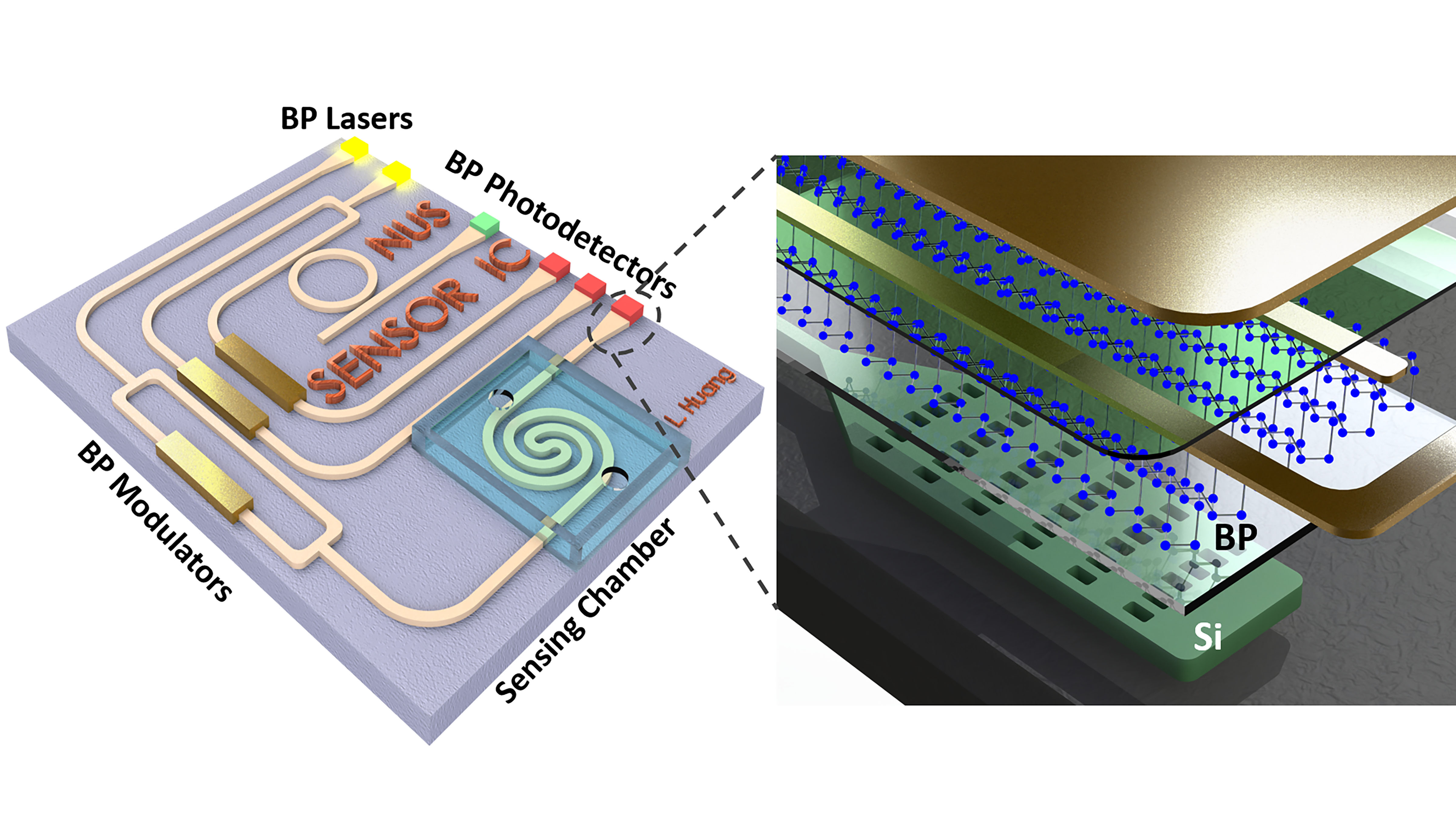
Black Phosphorus Future in 3D Analysis, Molecular Fingerprinting
Many compact systems using mid-infrared technology continue to face compatibility issues when integrating with conventional electronics. Black phosphorus has garnered attention for overcoming these challenges thanks to a wide variety of uses in photonic circuits. Research published in Applied Physics Reviews highlights the material’s potential for emerging devices ranging from medical imaging to environment monitoring, assessing progress in different components of the chips, from light detection to laser emission.

YOUNG INVESTIGATOR
Tingyi Gu, an assistant professor of electrical and computer engineering at the University of Delaware, has been selected for the Army Research Office Young Investigator Program. This prestigious award goes to early-career researchers pursuing fundamental research in areas relevant to the Army. Gu is studying materials that exploit the interface between light and electronics for potential use in lasers, displays, memory and more.
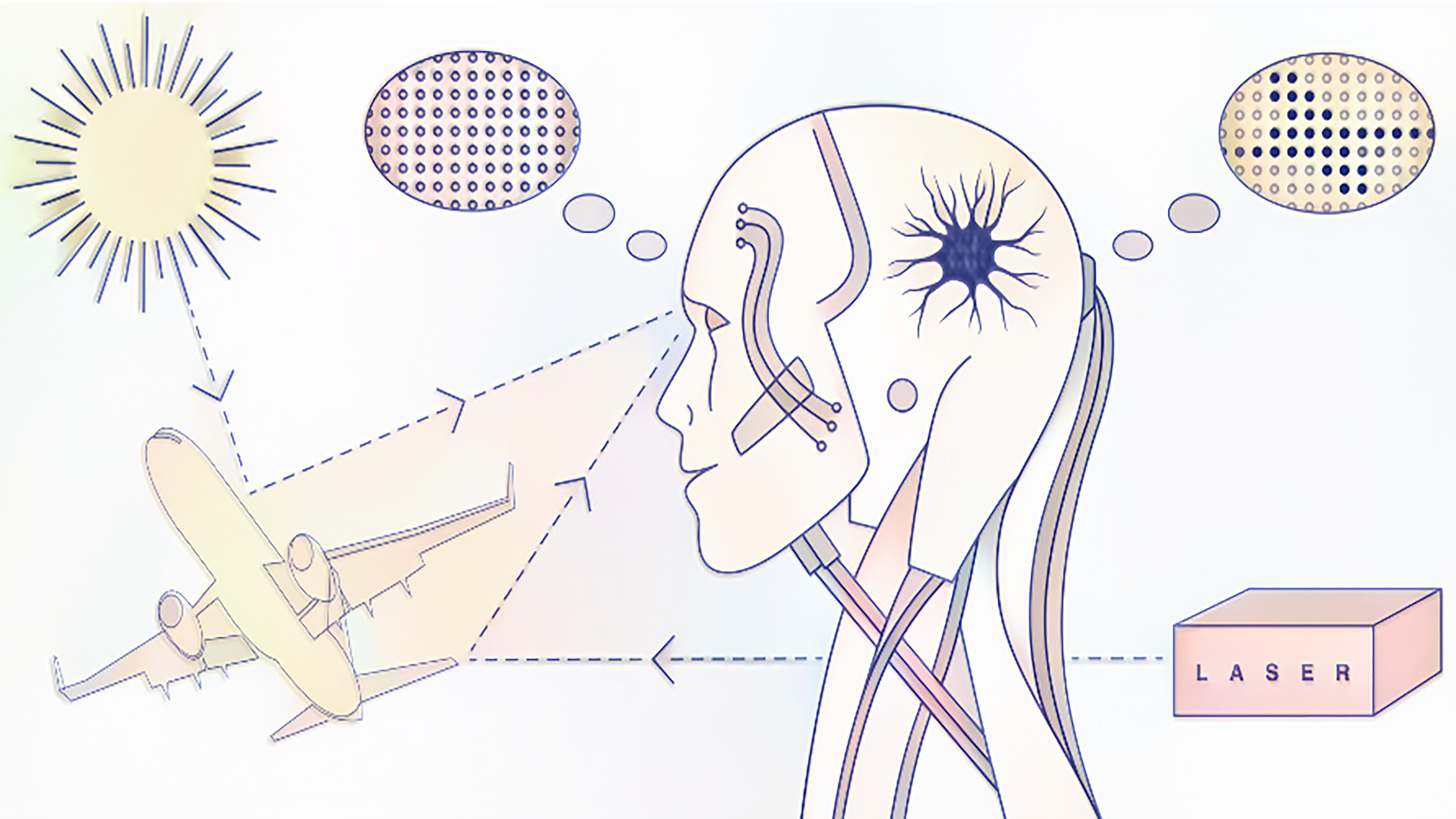
Identifying Light Sources Using Artificial Intelligence
Identifying sources of light plays an important role in the development of many photonic technologies, such as lidar, remote sensing, and microscopy. Traditionally, identifying light sources as diverse as sunlight, laser radiation, or molecule fluorescence has required millions of measurements, particularly in low-light environments, which limits the realistic implementation of quantum photonic technologies. In Applied Physics Reviews, researchers demonstrated a smart quantum technology that enables a dramatic reduction in the number of measurements required to identify light sources
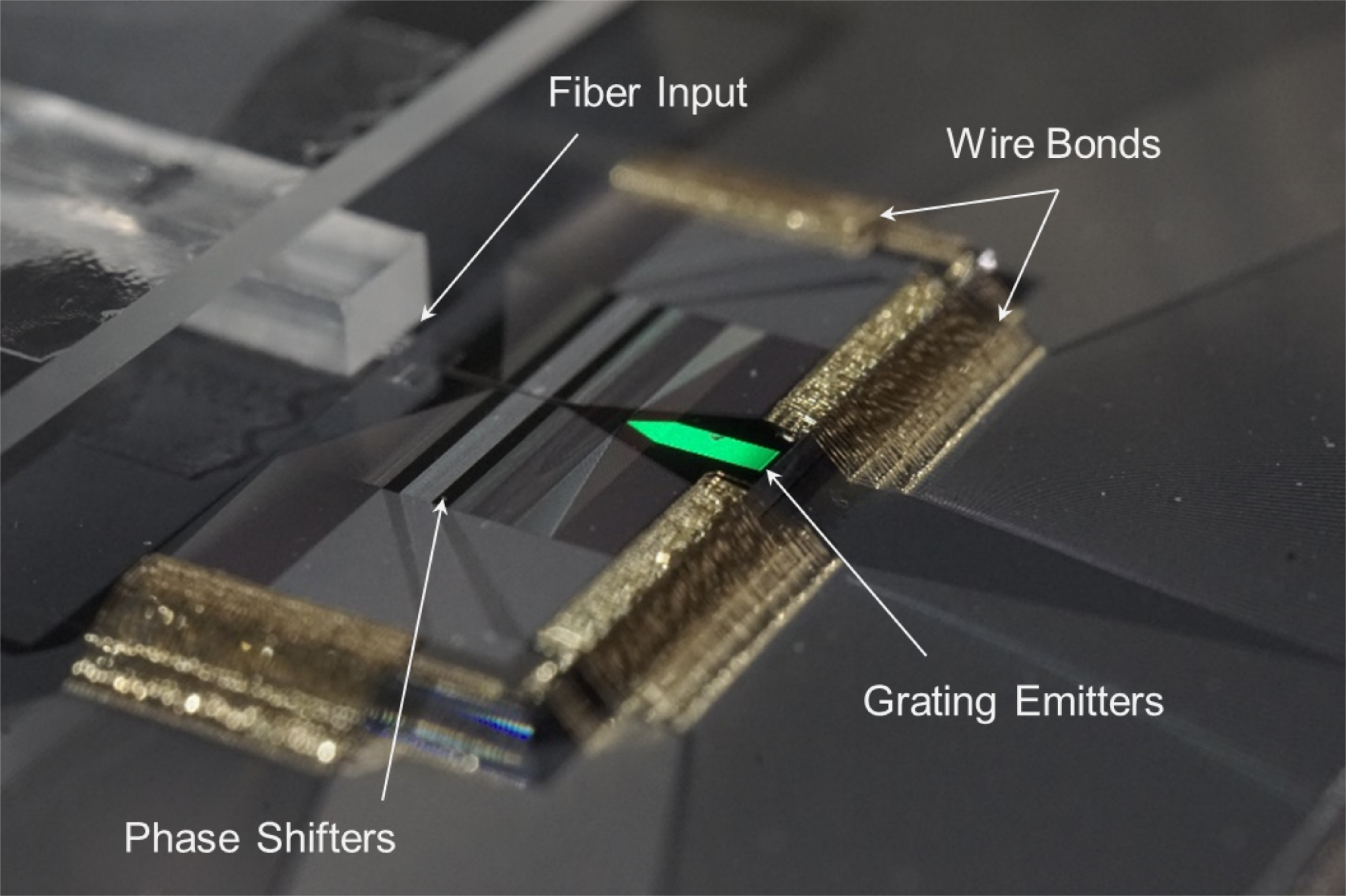
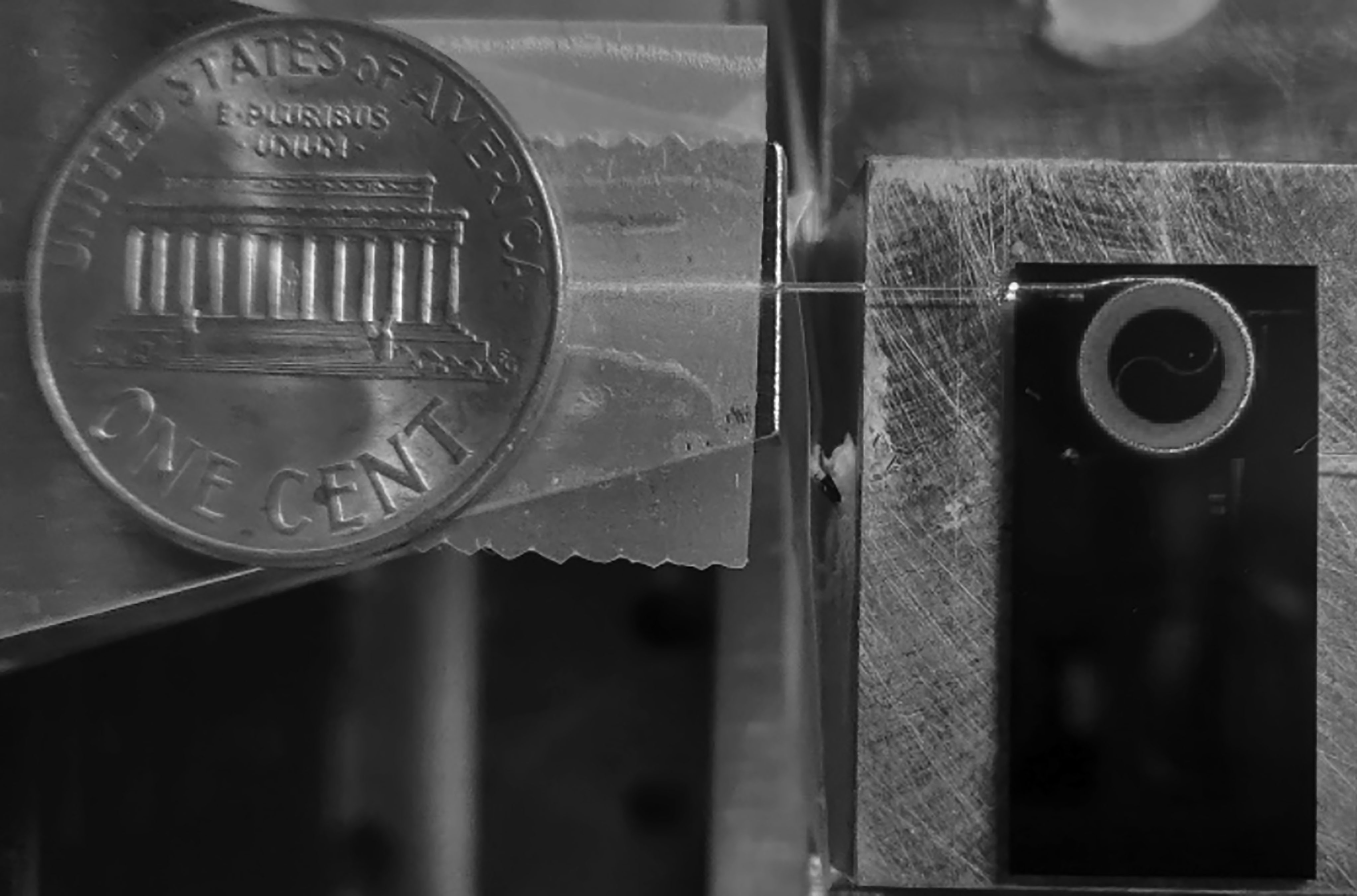
New Research on Compact Beam Steering Promises to Revolutionize Autonomous Navigation, Augmented Reality, Neuroscience
A Columbia Engineering team, led by Professor Michal Lipson, has developed a low-power beam steering platform that is a non-mechanical, robust, and scalable approach to beam steering.
Moving Precision Communication, Metrology, Quantum Applications from Lab to Chip
Photonic integration has focused on communications applications traditionally fabricated on silicon chips, because these are less expensive and more easily manufactured, and researchers are exploring promising new waveguide platforms that provide these same benefits for applications that operate in the ultraviolet to the infrared spectrum. These platforms enable a broader range of applications, such as spectroscopy for chemical sensing, precision metrology and computation. A paper in APL Photonics provides a perspective of the field.
UTEP Professor Named Fellow of International Society for Optics and Photonics
Raymond C. Rumpf, Ph.D., professor of electrical and computer engineering at The University of Texas at El Paso, was promoted to Fellow of the International Society for Optics and Photonics (SPIE), an educational nonprofit established to advance light-based science, engineering and technology.
Research at Argonne’s Advanced Photo Source Leads to New Ebola Drug
Scientists using specialized beamlines at Argonne’s Structural Biology Center (SBC), a facility for macromolecular crystallography at the Advanced Photon Source, derived insights that led to the discovery of a promising new drug for Ebola.