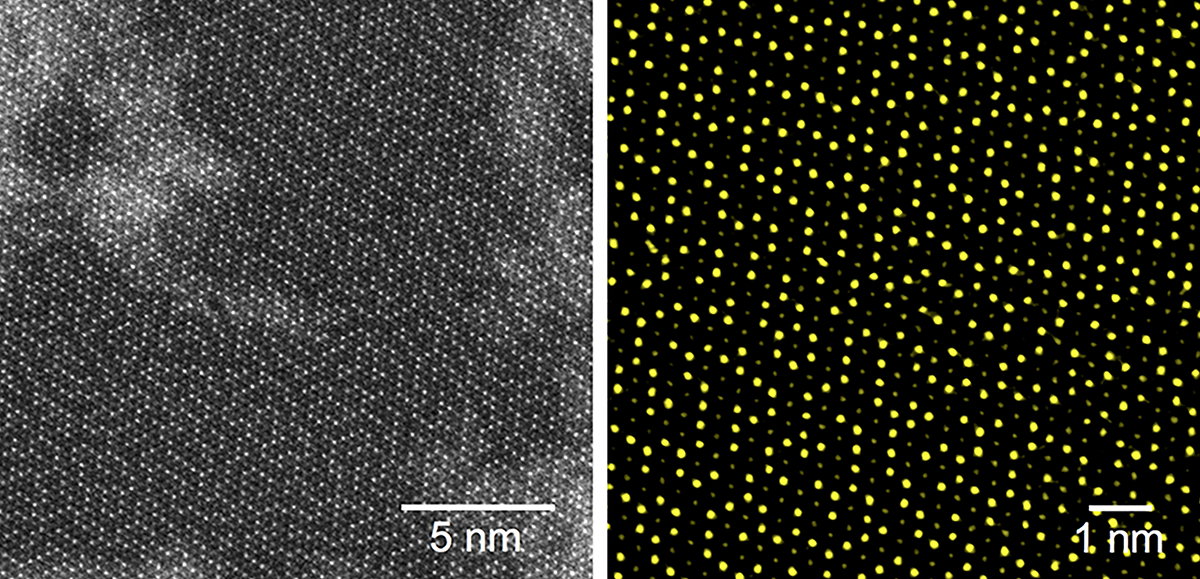
Scientists at Berkeley Lab have demonstrated a new technique that could improve the performance of atomically thin semiconductors for next-generation electronics such as optoelectronics, thermoelectrics, and sensors.

news, journals and articles from all over the world.

Scientists at Berkeley Lab have demonstrated a new technique that could improve the performance of atomically thin semiconductors for next-generation electronics such as optoelectronics, thermoelectrics, and sensors.

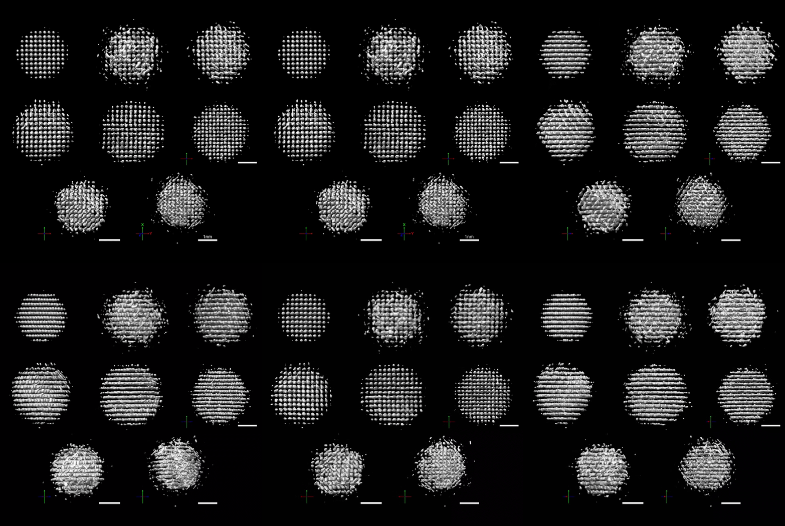
Researchers at Berkeley Lab have captured 3D images of nanoparticles in liquid with atomic precision, and developed an ultrathin electrical switch that could further miniaturize computing devices and personal electronics without loss of performance.
Columbia researchers have invented a new method—using ultraflat gold films—to disassemble vdW single crystals layer by layer into monolayers with near-unity yield and with dimensions limited only by bulk crystal sizes. The monolayers have the same high quality as those created by conventional “Scotch tape” exfoliation, but are roughly a million times larger. They can be assembled into macroscopic artificial structures, with properties not easily created in conventionally grown bulk crystals.