Ferroelectric materials can be found in different kinds of information processing devices, such as computer memory, transistors, sensors and actuators. Argonne researchers report surprising adaptive behavior in a ferroelectric material that can evolve step-by-step to a desired end, depending on the amount of photons from light pulses striking the material. Working alongside Argonne researchers were scientists from Rice University, Pennsylvania State University and DOE’s Lawrence Berkeley National Laboratory.
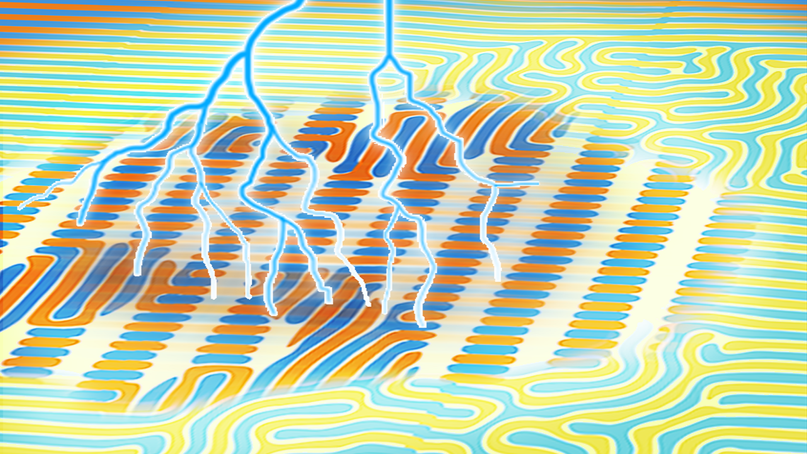
This team’s material is laden with networked islands or domains that are as distinct as oil in water. These domains are nanometers in size — billionths of a meter — and can rearrange themselves in response to light pulses. This adaptive behavior could be used in the energy-efficient movement of information in microelectronics.
The team’s ferroelectric sample is structured as a sandwich of alternating layers of lead and strontium titanate. Prepared by the Rice University collaborators, this seven-layer sandwich is 1,000 times thinner than a piece of paper. Previously, the team had shined a single, intense light pulse on a sample and created uniform, nanoscale ordered structures.
“Today’s supercomputers and data centers demand many megawatts of power. One challenge is to find materials for more energy-efficient microelectronics. A promising candidate is ferroelectric material that can be used for artificial neural networks as a component in energy-efficient microelectronics.” — Haidan Wen, Argonne physicist
“This time, we hit the sample with many weak light pulses, each of which lasts a quadrillionth of a second,” Wen said. “As a result, a family of domain structures, rather than a single structure, was created and imaged, depending on the optical dosage.”
To visualize the nanoscale responses, the team called upon the Nanoprobe (beamline 26-ID) operated by the Center for Nanoscale Materials and the Advanced Photon Source (APS). Both are DOE Office of Science user facilities at Argonne. With the Nanoprobe, an X-ray beam tens of nanometers in diameter scanned the sample as it was exposed to a barrage of ultrafast light pulses.
The resulting images revealed networked nanodomains being created, erased and reconfigured due to the light pulses. The regions and boundaries of these domains evolved and rearranged at lengths of 10 nanometers — about 10,000 times smaller than a human hair — to 10 micrometers, roughly the size of a cloud droplet. The final product depended on the number of light pulses used to stimulate the sample.
“By coupling an ultrafast laser to the Nanoprobe beamline, we can initiate and control changes to the networked nanodomains by means of light pulses without requiring much energy,” said Martin Holt, an X-ray and electron microscopy scientist and group leader.
The sample begins with a spiderweb-like arrangement of the nanodomains, and due to the disturbance created by the light pulses, the web breaks down and forms entirely new configurations that work in the service of some desired end in analogy to an adaptive network.
“We have discovered entirely new arrangements of these nanodomains,” said Stephan Hruszkewycz, an Argonne physicist and group leader. “The door is now wide open to many more discoveries. In the future, we will be able to test different regimes of light stimulation and observe even more unknown nanodomains and networks.” The power to visualize nanoscale change over time will be greatly improved with the recent upgrade to the APS, promising as much as 500 times brighter X-ray beams.
With this groundbreaking discovery of time-dependent changes in networked nanodomains, developers are on the path to building adaptive networks for information storage and processing. This advancement promises to create more energy-efficient computing systems.
This research is based on a paper in Advanced Materials. In addition to Wen, Holt and Hruszkewycz, authors include Marc Zajac, Tao Zhou, Tiannan Yang, Sujit Das, Yue Cao, Burak Guzelturk, Vladimir Stoica, Mathew Cherukara, John Freeland, Venkatraman Gopalan, Ramamoorthy Ramesh, Lane Martin and Long-Qing Chen.
Funding for the research came from the DOE Office of Basic Energy Sciences.
About Argonne’s Center for Nanoscale Materials
The Center for Nanoscale Materials is one of the five DOE Nanoscale Science Research Centers, premier national user facilities for interdisciplinary research at the nanoscale supported by the DOE Office of Science. Together the NSRCs comprise a suite of complementary facilities that provide researchers with state-of-the-art capabilities to fabricate, process, characterize and model nanoscale materials, and constitute the largest infrastructure investment of the National Nanotechnology Initiative. The NSRCs are located at DOE’s Argonne, Brookhaven, Lawrence Berkeley, Oak Ridge, Sandia and Los Alamos National Laboratories. For more information about the DOE NSRCs, please visit https://science.osti.gov/User-Facilities/User-Facilities-at-a-Glance.
About the Advanced Photon Source
The U. S. Department of Energy Office of Science’s Advanced Photon Source (APS) at Argonne National Laboratory is one of the world’s most productive X-ray light source facilities. The APS provides high-brightness X-ray beams to a diverse community of researchers in materials science, chemistry, condensed matter physics, the life and environmental sciences, and applied research. These X-rays are ideally suited for explorations of materials and biological structures; elemental distribution; chemical, magnetic, electronic states; and a wide range of technologically important engineering systems from batteries to fuel injector sprays, all of which are the foundations of our nation’s economic, technological, and physical well-being. Each year, more than 5,000 researchers use the APS to produce over 2,000 publications detailing impactful discoveries, and solve more vital biological protein structures than users of any other X-ray light source research facility. APS scientists and engineers innovate technology that is at the heart of advancing accelerator and light-source operations. This includes the insertion devices that produce extreme-brightness X-rays prized by researchers, lenses that focus the X-rays down to a few nanometers, instrumentation that maximizes the way the X-rays interact with samples being studied, and software that gathers and manages the massive quantity of data resulting from discovery research at the APS.
This research used resources of the Advanced Photon Source, a U.S. DOE Office of Science User Facility operated for the DOE Office of Science by Argonne National Laboratory under Contract No. DE-AC02-06CH11357.
Argonne National Laboratory seeks solutions to pressing national problems in science and technology by conducting leading-edge basic and applied research in virtually every scientific discipline. Argonne is managed by UChicago Argonne, LLC for the U.S. Department of Energy’s Office of Science.
The U.S. Department of Energy’s Office of Science is the single largest supporter of basic research in the physical sciences in the United States and is working to address some of the most pressing challenges of our time. For more information, visit https://energy.gov/science.