The Science
The Impact
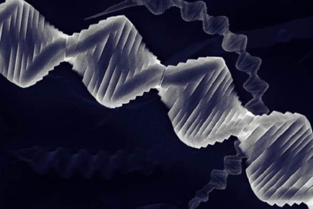
This is the first time that scientists have made 2D materials that form a continuously twisting shape in a structure that is thousands layers thick. The spiral structures could hold unique properties that aren’t observed in regularly stacked materials. Scientists could likely use this technique to grow layers of other materials that form atomically thin layers.
Summary
To create the twisted structures, the team took advantage of a crystal defect called a screw dislocation, a “mistake” in the orderly crystal structure that gives it a bit of a twisting force. This “Eshelby Twist”, named after scientist John D. Eshelby, has been used by others to create nanowires that spiral like pine trees. But this study is the first time the Eshelby Twist has been used to make crystals built of stacked 2D layers of an atomically thin semiconductor.
In a major discovery last year, scientists reported that graphene becomes superconductive when two atomically thin sheets of the material are stacked and twisted at what’s called a “magic angle.” While other researchers have since succeeded at stacking two layers at a time, this new work provides a recipe for synthesizing stacked structures that are hundreds of thousands or even millions of layers thick in a continuously twisting fashion.
By adjusting the material synthesis conditions and length, the researchers could change the angle between the layers, creating a twisted structure that is tight, like a spring, or loose, like an uncoiled Slinky.
Scientists performed X-ray analyses for the study at the Advanced Light Source and measured the crystal’s twist angles at the Molecular Foundry, both DOE Office of Science user facilities.
Funding
Y.L. and J.Y. are supported by the Samsung Advanced Institute of Technology. Work at the Molecular Foundry and the Advanced Light Source was supported by the Office of Science, Office of Basic Energy Sciences, of the US Department of Energy. H.S. and D.C.C. are supported by the US Department of Energy, Office of Science, Office of Basic Energy Sciences, Materials Sciences and Engineering. within the Electronic Materials Program (KC1201). This work was performed, in part, at the Center for Nanoscale Materials, a US Department of Energy Office of Science User Facility. We thank C. So, C. Song, X. Wang, S. Yan, K. Bustillo and C. V. Stan for help with the experiments.
Original post https://alertarticles.info


