The Science
The Impact
With this new approach, scientists can observe electrons’ spin properties at microscale. It also opens pathways for improving topological insulators and other conductive materials. Devices that operate on electron spin may have faster performance and lower energy consumption than conventional electronic devices that rely on charge. They could lead to new information storage, energy, and quantum information technologies.
Summary
Topological insulators are of growing interest to technology areas, especially quantum computing. They have unique surface properties that allow energy to be transported quickly and efficiently, without energy losses or temperature disruptions. Realizing their potential benefits, such as low-power energy consumption and high-speed data processing, requires scientists to have an in-depth understanding of the way electrons move through the surface of these unique materials.
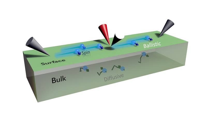
The bismuth-based topological insulator Bi2Te2Se can route electrons only through its surface and, theoretically, achieve ultrahigh conductivity. However, its performance has been limited in practice due to current leakage through the often-imperfectly insulating bulk interior. Researchers used novel scanning tunneling microscopy to investigate and control the intrinsic properties of Bi2Te2Se. For the first time, they measured “pure” spin transport close to the theoretical limit. This produced current with electron mobility an order of magnitude higher than reported before at the material’s surface on a micrometer-length scale.
The multiprobe technique was used to inject electrons only into the surface of the material and probe the spin-dependent portion of the current to achieve record high mobility. The results prove that it is possible to limit intrinsic properties that inhibit the material’s potential high conductivity. This work opens pathways to realizing devices that leverage these surface behaviors to develop transformative computing technologies.
Funding
The research was performed at the Center for Nanophase Materials Sciences, which is a DOE Office of Science User Facility, and supported by Korea’ Institute for Basic Sciences, the National Research Foundation of Korea, the Max Planck-POSTECH Center for Complex Phase Materials in Korea, and the U.S. National Science Foundation.
Original post https://alertarticles.info


