The Science
The Impact
This novel lens design will enable the next generation of ultrafast electron sources. These sources will in turn enable new characterization of materials and molecules. They will fill the gap in spatial resolution between static and ultrafast sources. This ability will allow scientists to characterize chemical dynamics at nanoscale dimensions of billionths of a meter.
Summary
Scientists have been using electrons to probe the structure of materials for decades. In recent years, researchers have manipulated electron beams to become small enough to study materials at the scale of individual atoms—and pulse fast enough to capture subtle atomic movements. However, they have had less success generating a beam that is both small and fast. Now, nanoscience researchers have created a new kind of electron source that has the potential to overcome this hurdle.
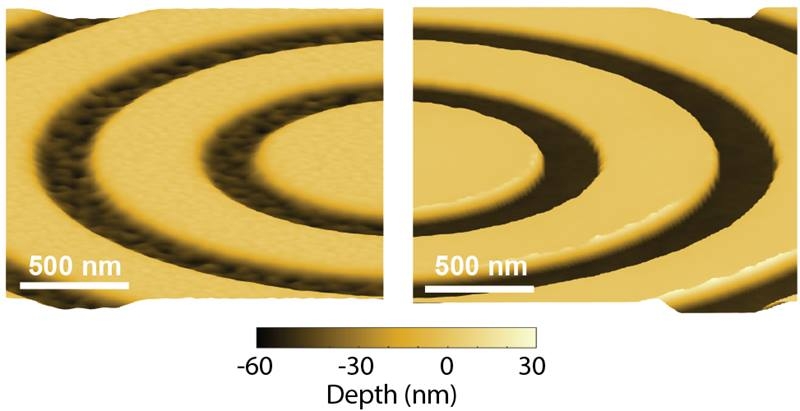
The electron source developed in this study is a gold surface with concentric circular grooves arranged in a bullseye pattern. When a laser hits the gold, the laser transfers energy to surface plasmons—electrons on the surface of the gold that move collectively. The bullseye’s grooves cause the plasmons to ripple inward and outward like waves bouncing off the sides of a pot of water. When the waves simultaneously hit the center of the bullseye, a small but intense beam of electrons fires out from the center. The response time of the source is less than 10 femtoseconds (the time it takes for light to travel 3 micrometers), and its size is approximately 100 nanometers (approximately the width of a cell membrane). For the emitted beam to be as bright as possible, the surface must be extremely flat. The researchers made an atomically flat surface using a new nanofabrication technique developed at the Molecular Foundry to enhance the beam brightness. The possibility of an ultrafast, tiny electron beam opens the doors for understanding chemical reactions and structural changes at molecular-length scales, particularly for materials such as nanoparticles that do not look the same over a large area or for interfaces between different materials.
Funding
The research was conducted at the Molecular Foundry and at the Berkeley Lab Accelerator Technology and Applied Physics Division. The research at the Molecular Foundry, a Department of Energy Office of Science user facility, was supported by the Office of Science, Basic Energy Sciences. Funding for the Berkeley Lab Accelerator Technology and Applied Physics Division research staff was provided by STROBE: A National Science Foundation Science and Technology Center.


