Researchers led by Prof. Dr. Mario Dähne (TU Berlin, Germany), Prof. Dr. Norbert Esser (TU Berlin and Leibniz Institute for Analytical Sciences, Germany), Prof. Dr. Frank Glorius (University of Münster, Germany), Dr. Conor Hogan (Institute of Structure of Matter, National Research Council of Italy, Rome, Italy) and Prof. Dr. Wolf Gero Schmidt (University of Paderborn, Germany) were involved in the study.
Technological miniaturization reaches its limits
“Instead of trying to artificially produce smaller and smaller structures with increasing effort, it is obvious to learn from molecular structures and processes in nature and to merge their functionality with semiconductor technology,” says chemist Frank Glorius. “This would make an interface, so to speak, between molecular function and the electronic user interface for technical applications.” The prerequisite is that the ultra-small molecules with variable structure and functionality would have to be physically incorporated with the semiconductor devices, and they would have to be reproducible, stable and as simple as possible.
Harnessing the self-organization of molecules
The self-organization of molecules on a surface, as an interface to the device, can perform this task very well. Molecules with a defined structure can be adsorbed on surfaces in large numbers and arrange themselves into a desired structure that is predetermined by the molecular properties. “This works quite well on surfaces of metals, for example, but unfortunately not at all satisfactorily for semiconductor materials so far,” explains physicist Norbert Esser. This is because in order to be able to arrange themselves, the molecules must be mobile (diffuse) on the surface. But molecules on semiconductor surfaces do not do that. Rather, they are so strongly bound to the surface that they stick wherever they hit the surface.
N-Heterocyclic carbenes as a solution
Being simultaneously mobile and yet stably bonded to the surface is the crucial problem and at the same time the key to potential applications. And it is precisely here that the researchers now have a possible solution at hand: N-heterocyclic carbenes. Their use for surface functionalization has attracted a lot of interest over the past decade. On surfaces of metals such as gold, silver and copper, for example, they have proven to be very effective surface ligands, often outperforming other molecules. However, their interaction with semiconductor surfaces has remained virtually unexplored.
Formation of a regular molecular structure
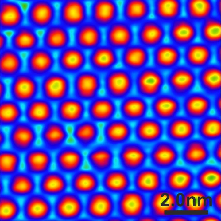
Certain properties of the carbenes are decisive for the fact that it has now been possible for the first time to produce molecular single layers on silicon surfaces: N-heterocyclic carbenes, like other molecules, form very strong covalent bonds with silicon and are thus stably bound. However, side groups of the molecule simultaneously keep them “at a distance” from the surface. Thus, they can still move about on the surface. Although they do not travel very far – only a few atomic distances – this is sufficient to form an almost equally regular molecular structure on the surface of the regularly structured silicon crystal.
Interdisciplinary collaboration
Using a complementary multi-method approach of organic chemical synthesis, scanning probe microscopy, photoelectron spectroscopy and comprehensive material simulations, the researchers clarified the principle of this novel chemical interaction in their interdisciplinary collaboration. They also demonstrated the formation of regular molecular structures in several examples. “This opens a new chapter for the functionalization of semiconductor materials, such as silicon in this case,” emphasizes physicist Dr. Martin Franz, first author of the study.
###
TThe study received financial support from the German Research Foundation (Leibniz Award; SFB 858, SCHM 1361/25), the Ministry of Culture and Science of North Rhine-Westphalia, the Governing Mayor of Berlin – Senate Chancellery Higher Education and Research, the German Federal Ministry of Education and Research, and the supercomputing centers of Stuttgart and Paderborn, and CINECA Italy (ISCRA initiative).
Disclaimer: AAAS and EurekAlert! are not responsible for the accuracy of news


