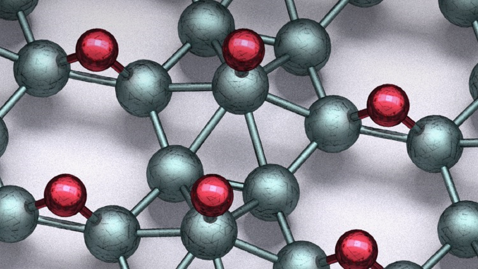
Scientists create stable nanosheets containing boron and hydrogen atoms with potential applications in nanoelectronics and quantum information technology.
What’s thinner than thin? One answer is two-dimensional materials — exotic materials of science with length and width but only one or two atoms in thickness. They offer the possibility of unprecedented boosts in device performance for electronic devices, solar cells, batteries and medical equipment.
In collaboration with Northwestern University and the University of Florida, scientists from the U.S. Department of Energy’s (DOE) Argonne National Laboratory report in Science magazine a breakthrough involving a 2D material called borophane, a sheet of boron and hydrogen a mere two atoms in thickness.
“We have tackled a significant challenge in determining the atomic structures from scanning tunneling microscopy images and computational modeling at the atomic scale with the help of computer vision.” — Argonne’s Maria Chan, nanoscientist at the Center for Nanoscale Materials.
One of the most exciting developments in materials science in recent decades has been a 2D sheet of carbon (graphene), which is one atom thick and 200 times stronger than steel. A similarly promising and newer material is an atom-thick sheet of boron, called borophene — with an “e.” A multi-institutional team, including researchers in Argonne’s Center for Nanoscale Materials (a DOE Office of Science User Facility), first synthesized borophene in 2015.
While graphene is simply one atomic layer out of the many same layers in the common material graphite, borophene has no equivalent parent structure and is very difficult to prepare. What’s more, the rapid reaction of borophene with air means it is very unstable and changes form readily.
“Borophene by itself has all kinds of problems,” said Mark Hersam, Professor of Materials Science and Engineering at Northwestern University. “But when we mix borophene with hydrogen, the product suddenly becomes much more stable and attractive for use in the burgeoning fields of nanoelectronics and quantum information technology.”
The research team grew borophene on a silver substrate then exposed it to hydrogen to form the borophane. They then unraveled the complex structure of borophane by combining a scanning tunneling microscope with a computer-vision based algorithm that compares theoretical simulations of structures with experimental measurements. Computer vision is a branch of artificial intelligence that trains high performance computers to interpret and understand the visual world.
Even though the borophane material is only two atoms thick, its structure is quite complex because of the many possible arrangements for the boron and hydrogen atoms. “We have tackled a significant challenge in determining the atomic structures from scanning tunneling microscopy images and computational modeling at the atomic scale with the help of computer vision,” said Argonne’s Maria Chan, nanoscientist at the Center for Nanoscale Materials. Given the success in unraveling this complex structure, the team’s automated analytical technique should be applicable in identifying other complex nanostructures in the future.
“What is really encouraging from our results is that we found a borophane nanosheet on a silver substrate to be quite stable, unlike borophene,” said Pierre Darancet, nanoscientist at Argonne’s Center for Nanoscale Materials. “This means it should be easily integrated with other materials in the construction of new devices for optoelectronics, devices combining light with electronics.” Such light-controlling and light-emitting devices could be incorporated into telecommunications, medical equipment and more.
“These findings are an important step in realizing borophane’s incredible potential as a two-dimensional material for nanoelectronics,” Chan said.
The scientific paper reporting this work, entitled “Synthesis of borophane polymorphs through hydrogenation of borophene,” appeared in Science. Authors are Q. Li, V.S.C. Kolluru, M.S. Rahn, E. Schwenker, S. Li, R.G. Hennig, P. Darancet, M.K.Y. Chan and M.C. Hersam.
This work was supported by the Office of Naval Research, the National Science Foundation, DOE Office of Basic Energy Sciences, and Laboratory Directed Research and Development funding from Argonne.
About Argonne’s Center for Nanoscale Materials
The Center for Nanoscale Materials is one of the five DOE Nanoscale Science Research Centers, premier national user facilities for interdisciplinary research at the nanoscale supported by the DOE Office of Science. Together the NSRCs comprise a suite of complementary facilities that provide researchers with state-of-the-art capabilities to fabricate, process, characterize and model nanoscale materials, and constitute the largest infrastructure investment of the National Nanotechnology Initiative. The NSRCs are located at DOE’s Argonne, Brookhaven, Lawrence Berkeley, Oak Ridge, Sandia and Los Alamos National Laboratories. For more information about the DOE NSRCs, please visit https://science.osti.gov/User-Facilities/User-Facilities-at-a-Glance.
Argonne National Laboratory seeks solutions to pressing national problems in science and technology. The nation’s first national laboratory, Argonne conducts leading-edge basic and applied scientific research in virtually every scientific discipline. Argonne researchers work closely with researchers from hundreds of companies, universities, and federal, state and municipal agencies to help them solve their specific problems, advance America’s scientific leadership and prepare the nation for a better future. With employees from more than 60 nations, Argonne is managed by UChicago Argonne, LLC for the U.S. Department of Energy’s Office of Science.
The U.S. Department of Energy’s Office of Science is the single largest supporter of basic research in the physical sciences in the United States and is working to address some of the most pressing challenges of our time. For more information, visit https://energy.gov/science.
