Producing structurally perfect graphene and other 2D materials is the secret to tapping into their potential novel electronic and spintronic properties. But how do we know when graphene, the most widely studied 2D material, is perfect– a defect-free and uniform layer of atoms?
Scientists at the U.S. Department of Energy’s Ames Laboratory have discovered an indicator that reliably demonstrates a sample’s high quality, and it was one that was hiding in plain sight for decades.
The researchers were investigating samples of graphene using low energy electron diffraction, a technique commonly used in physics to study the crystal structure of the surfaces of solid materials.
What they found didn’t follow the accepted rules of diffraction.
“The discovery is a paradox,” said Michael Tringides, a senior scientist at Ames Laboratory who investigates the unique properties of 2D materials and metals grown on graphene, graphite, and other carbon coated surfaces. “Textbook diffraction states that the more flawless a material is, the sharper and clearer the diffraction spots, and imperfect materials have low intensity, broader diffraction spots.”
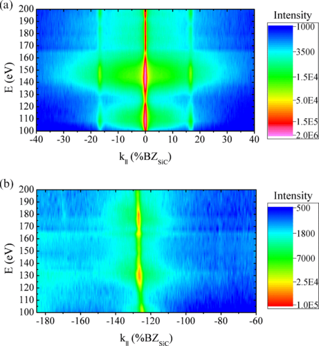
But in the case of highly uniform samples of graphene, the diffraction studies not only showed the expected sharp spots, but also a very broad band of diffuse diffraction in the background.
“That result is not intuitive and very strange,” said Tringides, “but we find this broad diffraction pattern to be an intrinsic feature to graphene, and when you have it, you have very good graphene. This is a good way to quantitatively measure its structural perfection.”
What’s more, this strange diffraction pattern was present and visible in the last 25 years of graphene research publications, and yet ignored. “It was a big, noticeable phenomena, and reproducible, and we realized it must be extremely important in some way,” said Tringides.
While more theoretical work is needed to fully explain the experimental findings, the scientists believe the broad diffraction phenomenon is caused by the confinement of graphene electrons within a single layer of atoms. According to the fundamentals of quantum mechanics, because the electron position normal to the layer is precisely known, their wave vector must have a spread, which is transferred to the diffracted electrons. This effect is significant for other types of 2D materials as well. With the continued and growing interest in 2D materials for a variety of applications, improving their structural quality will be the key to promising new technologies, said Tringides.
“This work provides an important step towards the ability to optimize graphene and other 2D materials precisely, and tailor their properties for specific applications,” he said.
The research is further discussed in the paper, “Diffraction paradox: An unusually broad diffraction background marks high quality graphene,” authored by S. Chen, M. Horn von Hoegen, P. A. Thiel, and M. C. Tringides; and published in Physical Review B.
Ames Laboratory is a U.S. Department of Energy Office of Science National Laboratory operated by Iowa State University. Ames Laboratory creates innovative materials, technologies and energy solutions. We use our expertise, unique capabilities and interdisciplinary collaborations to solve global problems.
Ames Laboratory is supported by the Office of Science of the U.S. Department of Energy. The Office of Science is the single largest supporter of basic research in the physical sciences in the United States, and is working to address some of the most pressing challenges of our time. For more information, please visit https://energy.gov/science.
Original post https://alertarticles.info
