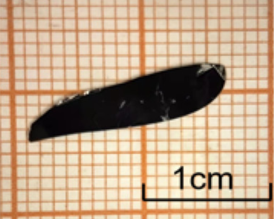
Scientists from Immanuel Kant Baltic Federal University in frames of academic mobility between China and Russia together with colleagues from Qiqihar University grew “defective” crystals of tin diselenide, that have atoms of selenium in greater or less amount, than in standard structure of this compound. It turned out that such crystals are able to conduct current better, than start material, and thanks to that they can become a promising base for creating optoelectronic devices, for example, photoconductors. Results of the research are published in the magazine Physics Letters. The work is chosen to be the feature story and put on the covers.
In every electronic device people use transistors – elements that are able to generate, intensify or transform electric current. Thus, for example, in photo conductors such components are necessary to transform light signals into electrical ones. One of promising materials for creation of high-production transistors is tin diselenide. Researches have shown that thanks to high mobility of current carriers – electrons – crystals on the base of that compound conduct current excellently, and also transform light impulses into electrical. Moreover, modelling have shown that electric, magnetic and optical properties of tin diselenide potentially can be managed, if you bring some defects into the material, in other words destruct its standard structure, extracting some atoms of selenium, or vice versa adding some extra ones. However as far as practical use is concerned, such effects haven’t been proved yet.
Scientists from Immanuel Kant Baltic Federal University (Kaliningrad) together with colleagues from Qiqihar University (China) grew in quartz tube crystallized compounds of tin diseledine. To achieve this aim, they at first heated particles of selenium and tin placed in tube up to 700°C, and then gradually cooled them to room temperature. Thanks to this temperature gradient they obtained crystals of “right” tin diselenide, that settled on walls of a tube, and also structures with shortage and abundance of selenium in the composition.
Authors compared outside appearance of obtained samples and found out that shortage and abundance of selenium influences the form of crystals’ edges. Thus, if on the face of the “proper” crystal there were even layers that formed the material, whereas in the condition of shortage of selenium layers had irregular shape. When there was an abundance of selenium, layers can’t even be recognized – they were substituted by disorderly placed structures on the surface, that remind folds.
Besides this, “proper” and “defective” crystals correlate with laser light differently. Thanks to different absorbance spectrum, “defective” crystals potentially can be used in construction of transmitters, the absorbance spectrum of which doesn’t correspond to maximums in spectrum of a usual tin diselenide.
Estimation of electrical properties of samples showed, that crystals with defects have forbidden energy region in 1.5-2 times smaller than “proper” tin diselenide. The size of the forbidden region shows how well a material can conduct current. Thus, the smaller a forbidden region the better conductor a material is. Therefore, conducting properties of crystals with shortage and abundance of selenium turned out to be better, than starter compound. It proves the fact that “defective” materials can show higher efficiency in usage as a base for optoelectronic devices.
“Training in China for me was a unique opportunity to acquire an experience of work with foreign scientists. Together with my Chinese scientific supervisor and other researchers we worked on obtaining defective crystals of tin diselenide, that can become promising photoconductor”, – tells Vera Ni, master’s student of SEC Smart Materials and Biomedical Applications Research Centre of Immanuel Kant Baltic Federal University.
“In future we plan to predict new possible structures and model their properties in connection with the experiment. We plan in our work to continue close cooperation with Qiqihar University”, – tells Kurban Magomedov, research officer of SEC Smart Materials and Biomedical Applications Research Centre of Immanuel Kant Baltic Federal University.
