In particular, 2-D perovskites sandwiched in between large organic molecules—which act as spacers in the perovskite crystal lattice—have attracted a lot of interest not only because of their low-cost manufacturability but also their enhanced optoelectronic properties. The high color purity, tunability, and brightness of 2-D layered perovskites make them promising materials for next-generation lighting and displays. In addition, the external quantum efficiency of perovskite-based LEDs—the ratio of the number of light particles emitted from the device to the number of electrons passing through the device—has been rapidly improving.
Now, a team led by the U.S. Department of Energy’s (DOE) Los Alamos National Laboratory in collaboration with Brookhaven and Argonne National Laboratories has demonstrated that the choice of organic spacer significantly impacts LED performance. By using organic spacers with atoms arranged in a ring instead of a linear chain, the scientists increased device efficiency by two orders of magnitude (to around 12 percent) and brightness by 70 times, with a luminance approaching that of typical green organic LEDs.
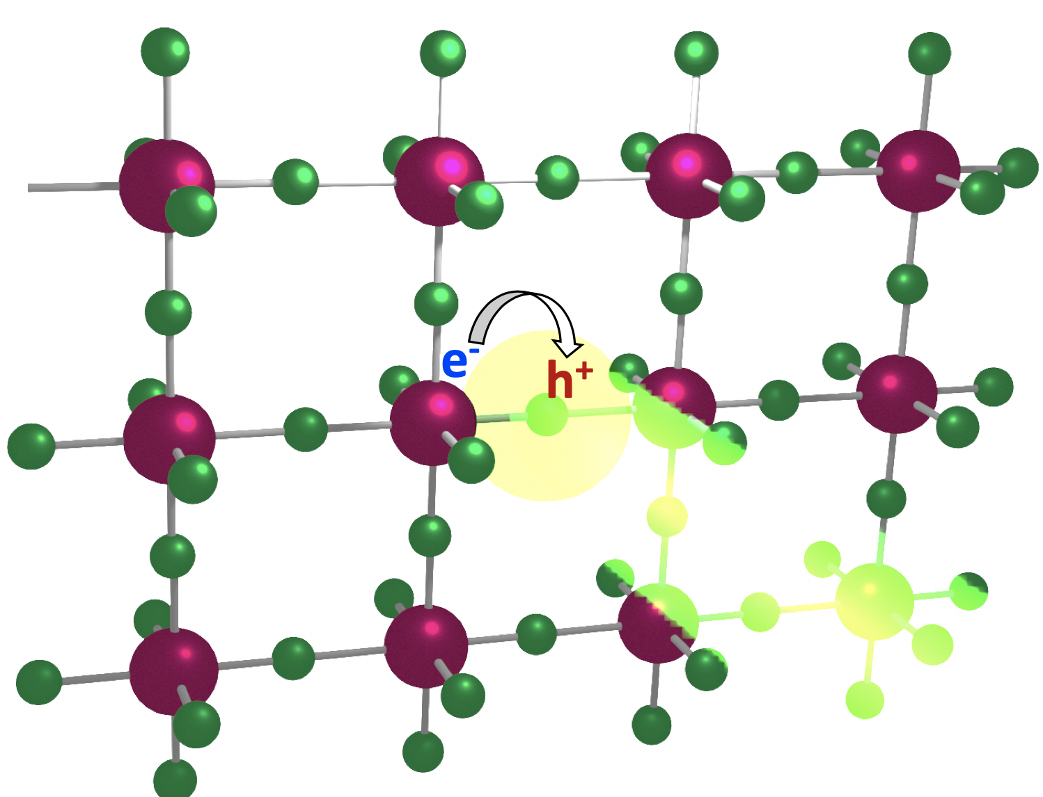
“The large organic spacers slice the 3-D perovskite crystal lattice into a 2-D layered structure consisting of graphene-like atomic sheets each less than a billionth-of-a-meter thick,” explained Wanyi Nie, a scientist at the Center for Integrated Nanotechnologies (CINT) at Los Alamos.
In this case, the scientists compared LEDs based on 2-D lead bromide perovskites with alkyl (linear) or benzyl (ring) organic spacers. To ensure a fair comparison between the two types of devices, Nie and Hsinhan (Dave) Tsai—a J. Robert Oppenheimer Distinguished Postdoc Fellow at Los Alamos—first synthesized high-quality materials and fabricated highly crystalline thin films of the perovskites under the same processing conditions. Then, they validated the films’ crystalline structure and orientation through electron microscopy and x-ray scattering.
Next, the team studied the films’ light emission (photoluminescence) properties at Brookhaven’s Center for Functional Nanomaterials (CFN) and Argonne’s Center for Nanoscale Materials (CNM).
At the CFN Advanced Optical Spectroscopy and Microscopy Facility, staff scientist Mircea Cotlet and research associate Mingxing Li of the Soft and Bio Nanomaterials Group measured the photoluminescence decay of the films after excitation with a light pulse.
“Called time-resolved optical microscopy, this technique allows us to measure the rate at which electrons and holes recombine, in turn giving us information about charge-carrier lifetimes,” explained Cotlet.
“Our measurements showed that light-excited carriers in the benzyl perovskite have a lifetime five times longer than that of the alkyl perovskite,” said Li.
The extended carrier lifetimes increased luminescence efficiency, resulting in brighter light emission from the benzyl perovskite.
At CNM, staff scientist Xuedan Ma applied high-resolution scanning laser microscopy to map the spatial distributions of the photoluminescence from the films. This mapping revealed that the benzyl perovskite thin films had a stronger, more uniform emission intensity.
“We observed quite substantial differences in the emission intensities and distributions of the different types of films, which could be attributed to the distinct carrier dynamics in the materials,” said Ma.
To link these photophysical properties with electronic structure dynamics, Xiaoyi Zhang’s team at Argonne’s Advanced Photon Source (APS) performed time-resolved x-ray absorption spectroscopy.
“This method relies on the unique timing structure and powerful single x-ray pulses of the APS to track very small changes that happen very quickly,” said Zhang. “The time-resolved x-ray absorption technique itself is highly sensitive to the charge changes, so it can tell us absolutely where the charge is and how it flows inside the material.”
The spectra showed a change in the electronic structure on the bromide sites of the benzyl perovskite only.
“The holes on the bromide sites don’t immediately get stuck in charge traps, or electronic defects in the material,” explained Tsai. “The holes can wait around for electrons to show up and recombine to generate light instead of wasteful heat. This phenomenon is related to the 2-D crystal structure of the material. The rigid, bulky benzyl ring affects the crystalline packing of the perovskite, thereby changing the charge transport and recombination processes.”
Back at Los Alamos, Nie and Tsai assembled the thin films into LEDs and measured device efficiency and brightness. In a final demonstration, they performed an operational lifetime test of the benzyl perovskite-based LED. Under continuous operation with a high injection current and in ambient conditions, the device lasted 25 minutes.
“Compared to organic LEDs, which can last 100,000 hours, 25 minutes may seem short,” said Nie. “But it is an improvement if you consider that perovskites are only just beginning to be researched and they tend to be sensitive to various external conditions such as humidity and applied voltages. This advance brings us one step forward toward more stable perovskite-based LEDs.”
In follow-on studies, the team will determine whether embedding the 2-D perovskites inside an organic matrix could help prevent degradation. They will also explore other organic spacers that may enhance the charge recombination effect.
“Because of their low-cost manufacturability and desirable optoelectronic properties, 2-D perovskites are exciting not only for LEDs but also for other applications,” said Tsai. “These light-emitting materials could be useful for x-ray medical imaging, optical communications, and lasing, for example.”
This research—published in Advanced Science on Feb. 19—was in part supported by the Laboratory Directed Research and Development program, Quantum Initiative funding, and J. Robert Oppenheimer Distinguished Postdoc Fellowship at Los Alamos. The x-ray absorption spectroscopy studies used resources of the sector 8-ID-E and 11-ID-D beamlines at APS, a DOE Office of Science User Facility. The CFN, CINT, and CNM are also DOE Office of Science User Facilities and Nanoscale Science Research Centers.
Brookhaven National Laboratory is supported by the U.S. Department of Energy’s Office of Science. The Office of Science is the single largest supporter of basic research in the physical sciences in the United States and is working to address some of the most pressing challenges of our time. For more information, visit https://energy.gov/science.
Follow @BrookhavenLab on Twitter or find us on Facebook.
Original post https://alertarticles.info