The Science
Semiconductors can respond to heat or light to convert one form of energy to another. Combining two different semiconductors creates useful properties for devices. The way these combinations work depends on how the semiconductors are arranged and contact one another. Researchers have developed a new way to grow semiconductor crystals about 100,000 times smaller than the width of a human hair. These semiconductor crystals grow on similarly sized forms of a different semiconductor. This new synthesis method independently controls the arrangements and sizes of the crystals.
The Impact
Researchers can achieve advanced properties for functional devices only if the materials are the right size and in the right arrangements. This research showed how one semiconductor arranged itself as nanocrystals in response to the surface structure of another. The final sizes of the crystals were easy to control. These structures are much more intricate than the flat layers of semiconductors in conventional transistors. This ability to control their formation could lead to new applications, for example as sensors and catalysts, further advancing nanoscience.
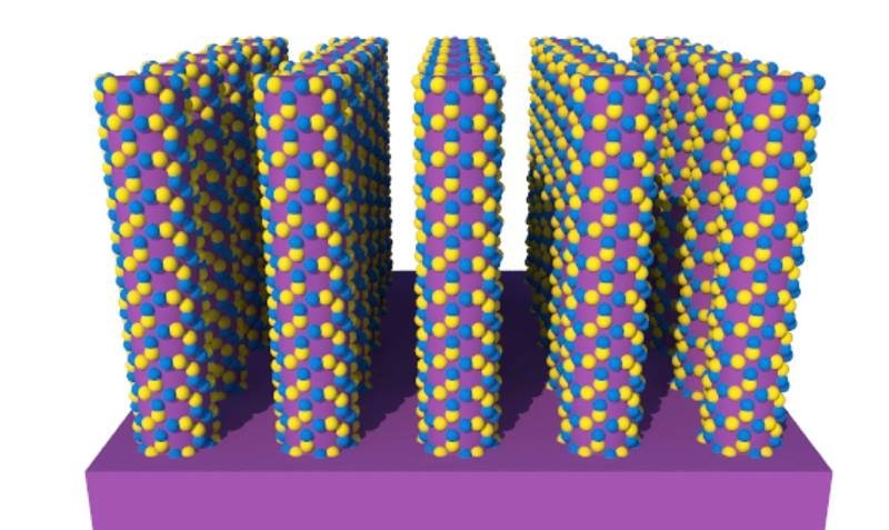
Summary
Researchers formed semiconductors from different components by adding one atomic layer at a time. They grew nanocrystals of zinc oxide on molybdenum disulfide surfaces in precise arrangements and sizes. These materials could be used in sensors and catalysts. The structures were created by first depositing molybdenum trioxide films. Chemical reactions converted these to molybdenum disulfide films. Higher temperatures produced more ordered films with fewer defects. Repeated cycles of atomic layer deposition placed zinc oxide atoms on the films. The researchers monitored changes in the new material’s order and nanocrystal growth during this process. The arrangements of the nanocrystals were determined by the pattern of defects on the molybdenum disulfide. These methods also were used to grow zinc oxide nanocrystals on three-dimensional molybdenum disulfide nanowires. This new advance creates semiconductor materials in ways that are predictably controlled by the synthesis process.
Funding
The work was supported primarily by the Department of Energy Office of Science, Basic Energy Sciences, Materials Sciences and Engineering Division and made use of the Stanford Synchrotron Radiation Lightsource, a DOE Office of Science User Facility. The research also used the Stanford Nano Shared Facilities supported by the National Science Foundation.
Additional support was provided by: the National Research Foundation of Korea (for synthesis and theoretical calculations), Ministry of Trade, Industry and Energy, and the Korea Semiconductor Research Consortium (for devices), the Netherlands Organization for Scientific Research (for post-doctoral fellowship support), and the European Union’s Horizon 2020 Research and Innovation Programme (for post-doctoral fellowship support).